Nvidia Pascal Speculation Thread

Status
Not open for further replies.
Biggest question on my mind:

With Pascal probably becoming a reality in 2017 for Nvidia's GeForce gaming products, will AMD's equivalent Radeon GPUs (and APUs) with stacked DRAM, ( be it 2.5D or 3D stacking) likely to be also implemented in the semi custom APUs for the future next generation consoles in 2018/2019, assuming AMD gets those console design wins?

I don't see why not.
 
I do: as a replacement for SLI.

Agreed.

I wonder if the motherboard makers can implement multi-GPU NVLINK connectivity themselves, perhaps without fast main memory access?

Also it would be especially feasible on the dual GPU systems where the two chips are connected via a PCIe switch today. There NVLINK really makes sense because such a solution would have the potential for much better scaling (it would appear as one huge GPU from the outside world).
 
I'm hoping the big pascal will be the worlds first 20 teraflop GPU.

If the big maxwell turns out to be about 7 teraflops and the 16nm node can allow for three times the transistor density I think it is possible.
 
I'm hoping the big pascal will be the worlds first 20 teraflop GPU.

If the big maxwell turns out to be about 7 teraflops and the 16nm node can allow for three times the transistor density I think it is possible.

16nm allows roughly double the transistor density over 28nm. You forget that 20nm to 16nm is essentially no increase in density.
 
According to TSMC's latest claims it does provide a 10~15% increase in density. Not great, but not insignificant either.
 
According to TSMC's latest claims it does provide a 10~15% increase in density. Not great, but not insignificant either.

Sorry I should have been a bit more clear. I was talking about the first 16nm process, i.e. 16 FF. 16FF brings at max a ~5% increase over 20SoC.

That 15% figure is for 16FF+ compared to 16FF.
 
Last edited by a moderator:
The number (15 %) isn't related to density, but speed (16nm FF+ should reach ~15 % higher clocks than 16nm FF - density will stay at the same level, I believe).
 
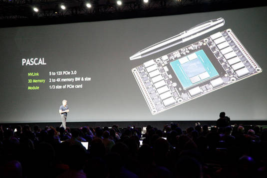
Besides being small and very power-efficient, it will be amazing if they are able to stack modules in the picture "on top of each other" ... assuming 3D packaging containers and NVLink advance enough to allow that capability. It would make for an extremely scalable architecture.

Additional comments from Huang regarding picture on first page ....
Pascal: 'A supercomputer the size of two credit cards,' Huang says

He did, however, promise big things for Pascal, displaying a small card with a prototype Pascal chip onboard. "This little module here," he said, "represents the processor of next-generation supercomputers, next-generation workstations, next-generation gaming PCs, next-generation cloud supercomputers." A tall order, to be sure, but if the dual promise of NVLink and 3D packaging comes through, Huang just might have a small, power-efficient, high-bandwidth winner on his hands.
pascal.jpg


IBM seems to be jumping on the bandwagon ...

It also plans to keep working with Nvidia as its exclusive partner on its GPU acceleration efforts. The next generation of Power8 servers will incorporate Nvidia's NVLink technology, which speeds up data exchange between the CPU and GPU, although those servers won't be ready until at least 2016.
http://www.theregister.co.uk/2014/10/03/ibm_and_nvidia_team_on_power8_servers/
 
IBM should have been happy this day be called bandwagon, when Nvlink, if on the Nvidia side developped in collaboration with IBM, is purely and simply an IBM things. (( that Nvidia will use so. ) But IBM is not the first and not the last on this, every server / computing enterprise are now developping link for replace DirectGMA and other stuff equivalent to what Nvidia is calling "nvlink" .. I see Nvlink as a direct follow of DGMA. ( AMD DGMA ).. but sadly like in all this roadmap what we see is " what will come next".. Like if Nividia wanted to be sure to be the first to announce it during this sessions.. HBM ( who are developped between SK Hynix and AMD and will surely come before on AMD gpu's ), NvLink ( as i have write the follower of DGMA is allready on the road for it ), etc etc .

NvLink is nothing special, every HPC company are now and still a long time at work for provide the same things.. if IBM was working on this, thats not a mistery and i can ensure you that it will not be so much different of what other have to offer on this aspect. ( they was just the first to put it in a roadmap ). And i can ensure you that AMD have allready the same type of link in preparation since a long long time before this was annonced.
 
Last edited by a moderator:
AMD needs a greatly revamped GPU architecture to make this work. IMHO the current/near future architecture is way too inefficient (power/heat) for stackable GPU/Memory solutions unless their future plans point to using hybrid (water) cooling solutions for everything.
 
AMD needs a greatly revamped GPU architecture to make this work. IMHO the current/near future architecture is way too inefficient (power/heat) for stackable GPU/Memory solutions unless their future plans point to using hybrid (water) cooling solutions for everything.

It's not like NVIDIA needed one to bring what was Fermi to what now is Maxwell, sure there were changes but no "major overhauls" completely changing the architecture
 
AMD needs a greatly revamped GPU architecture to make this work. IMHO the current/near future architecture is way too inefficient (power/heat) for stackable GPU/Memory solutions unless their future plans point to using hybrid (water) cooling solutions for everything.

Maxwell is really efficient for do what she need to do in the game department.. for the rest, im not so sure... Understand me, i really like what Nvidia have done with Maxwell in term of efficiency, but the road dont end there ..
 
Last edited by a moderator:
Besides being small and very power-efficient, it will be amazing if they are able to stack modules in the picture "on top of each other" ... assuming 3D packaging containers and NVLink advance enough to allow that capability. It would make for an extremely scalable architecture.
That was not promised, just the stacked memory.
Stack a module on the other, and it's stacking a full PCB, a multi-hundred Watt GPU, and all those hot VRMs right on top of each other.
(addendum: The full PCB is admittedly small, but it's still a thermal barrier if nothing else.)
 
Maxwell is really efficient for do what she need to do in the game department.. for the rest, im not so sure...
Why would it be less efficient for compute? Nvidia claims that the SMs saw a 2x efficiency increase, which is what gets hammered the hardest in compute.

And if you read the CUDA dev forum discussion that spworley linked to a few days ago in the Maxwell thread, you'll see that the compute results are very similar in terms of power.

in what SP compute ? SGEMM ? seriously ? Again i admire what have done Nvidia in the department of efficiency, bringing a boost on performance who can be allocated to shrink of process by increasing the CUDA cores efficiency.. but like i have said, this is not the end of the road.
 
Last edited by a moderator:
Status
Not open for further replies.
Back
Top