*Hiroshige's Goto Weekly overseas news*
GPU of the WGF2.0 generation where operation above 1GHz becomes possible
--------------------------------------------------------------------------------
- Separation of programmable unit advances with fixed function
In WGF2.0 generation GPU, the coherence of Shader increased, the fact that the possibility the Shader array where architecture was standardized even physically being mounted is high the last time was explained. One of advantage of this architecture is Shader load balancing. But is not just that. Also the performance improvement with the high clock conversion of GPU, is the important point.
In WGF2.0 generation GPU, it can accelerate GPU theoretically substantially. Because that compared to time speed can convert the Shader core of GPU until now easily. Because of that, while GPU which operates above internal 1GHz is close there is a possibility of appearing.
Current DirectX 9 generation GPU is designed to be the structure where the fixed functional part and the Programable Shader part which has program characteristic are complicated. In the DirectX 9 generation as for fixed function it is to be reduced, in the WGF2.0 generation furthermore the fixed functional part is decreased, but fixed function remains as still. Because as for this, fixed functional one, directly is more efficient processing than programmable unit.
As for Programable Shader if with the same programmable operational unit as CPU, it turns fast, that much efficiency rises. In addition, operational unit itself is not to mount complicated logic with ハードワイヤド, basic operational logic is mounted because of general purpose. Because of that, acceleration by any chance inhaling. It has the character which is similar to CPU.
Vis-a-vis that, the fixed functional part has mounted the logic for specification processing as ハードワイヤド. When logic becomes complicated, speaking generally, it is difficult to increase clock frequency. On the other hand, because logic is hard converted that way, the to high clock it cannot convert and can process also the て fast. If "with Shader several cycles the processing which catches, hardware mounting it can execute in 1 cycle. The efficiency per プログラマビリティ and cycle there is a relationship of trade-off ", that a certain GPU authorized personnel talks.
In other words, as for the fixed functional part as for high clock conversion it is difficult, but it can put out efficiency low even with the clock. On the one hand, if as for Shader the same clock efficiency falls from ハードワイヤド, but it means that high clock conversion is easy.
- Clock domain of the Shader core part is designated as 2 time speed
GPU this way, has loaded together the unit where character differs, so far being dragged to the fixed functional part, it was difficult to lift the clock. GPU remained always in operational frequency of 1 of several parts of CPU, parallelism was largely detached being high, at frequency. As for this, same even in the DirectX 9 being generation GPU, as for GPU extent it is distant in the GHz stand. As for this, with special care Shader, the fact that original efficiency cannot be shown is meant. For example, when it tries that GPU of 500MHz will achieve the same logical peak efficiency as Cell which can operate 8 SIMD processors with 4GHz, 64 Shader must be placed.
But, when it becomes WGF2.0 generation architecture, this problem reaches the point where it can solve partly. In WGF2.0 generation GPU, it is presumed that it collects Shader where many GPU vendors are the programmable operational core as コンピ…テーションコアアレイ. With mounting such as that, it is easy to separate Shader from other unit.
When it does, just Shader array separating clock domain, the question っ callous which is operated with the clock of 2 times that other unit becomes easy. For example, as for the whole GPU with also 600MHz operation, to operate with 1.2GHz it can do Shader array. It means that the operational efficiency of Shader rises rapidly.
Separation of such clock domain in the device of SOC type is done to popular. For example, as for the PSP tip/chip the CPU core is operational with time speed of other unit.
Of course, for that, Shader, from it is necessary to modify in the design which subdivides the pipeline. In addition, because as for accelerating with just the operational efficiency of Shader does not rise, as for other efficiency, when the bottleneck are other things, either entire efficiency does not rise. But, it reaches the point where operational efficiency with respect to theory can lift at least more easily. Whether or not time fast core appears in the first generation of WGF2.0 generation GPU, it is not understood, but GPU where Shader operates above 1GHz appears probably will be in the WGF2.0 generation.
The clock of GPU of WGF2.0 age
As for PDF editionthis
- In the possibility the design of GPU changing in the long term
When Shader operational efficiency rises, there is a possibility also the design philosophy of GPU changing. As for former GPU, in order to be able to increase efficiency with also the relatively low clock, it faced to the direction which increases the degree of parallel of processing. The quantity of Pixel Shader 4 -> increased at 8 -> 16 and many fold, GPU itself had enlarged because of that.
But, in the future, when we assume that most to be required with Shader efficiency, as for Shader efficiency itself can lift with time fast conversion of the core the inevitability which increases the quantity itself of Shader fades. For example, if even with same Shader quantity 12 as the mid range GPU of present condition, it operates with time speed, per 1 clock operation of 24 Shader minute becomes possible. Because of that, with GPU below mid range as for the spirit which increases parallelism there is also a possibility of becoming dull. Though, just the high end for efficiency demand for the ceiling not knowing, the possibility of keeping raising parallelism as still is high, but.
There is a possibility also approach itself of the design of GPU changing. The design period of present GPU at the half of CPU, from development start the product appears in the market in 18 - 24 months. Because with GPU, custom in the circuit design チ…ーン it does not do in acceleration that time is not required for the design. For example, David B. of NVIDIA Kirk (the デビッド B kirk) the person (Chief Scientist), you talked the reason as follows 3 years ago.
If チ…ーン it does "in the custom design, (GPU) as for more becoming high speed is certain. Problem is that time is required for the design. For example, after with CPU of Intel and the like, アーキテクチャデザイナ finishing work, also approximately 1 - 2 years spend time on transistor tuning. When the same thing it is GPU, in 2002, it means to put out TNT2 of 2GHz ",
In other words, with GPU addition of hardware specification and change of architecture are extremer than CPU. Because of that, when it is necessary to turn the design shortly in the cycle, so does, it is the case that for accelerating チ…ーン how you had not been able to have done in the custom design.
But, the technical trend of GPU is changing largely. New specification is not to add with the hardware, it actualizes with the software on Shader. Because of that, with flexible it has been about it will make Shader as much as possible in general purpose and to change. And, GPU efficiency is reaching the point where it depends on the acceleration of Shader. So when it does, if the architecture whose as for the GPU manufacturer is widely used in principle you spend time on the design, チ…ーン do in the high clock and you reach the point where it corresponds. Perhaps until recently it keeps changing to the development cycle which differs.
When that happens, like the CPU manufacturer high speed the processor core is designed and the development position which is accustomed, the possibility of embarking on GPU development comes out. Actually, in the past, the authorized personnel of a certain CPU vendor talked the idea such as that. If approach of the CPU design is introduced, because from high speed it is possible, to make GPU, you said that you have proposed to the parent company.
In addition, even with the next generation PlayStation, there was also a project of the GPU development which designates the Cell processor as the base. If Programable Shader is made in the SPE base and the luster riser and ポストシェーダ processing unit etc. are mounted with fixed function, that is the expectation which with that has become epoch-making GPU. In the future, more and more, there is a possibility seamless conversion of the design of such CPU and GPU advancing.
- The mounting Geometry Shader which designates the common hard conversion of Shader as prerequisite?
The WGF2.0 generation GPU where structure changes on the Shader center. As for this change, more drastic function, means the fact that the possibility of keeping being mounted in the form which is actualized with Shader is high. What it suggests that is Geometry Shader and "Tessellator (plane surface divided unit)".
Geometry Shader is the Shader stage which joins anew with WGF2.0. It has become the operation stage which ジオメトリシェーダ which handles the primitive (is also the times when it is called プリミティブシェーダ and) can send the program.
As for the difference with Vertex Shader which is in the same geometry pipe, as for Vertex Shader do the processing of the primitive unit. It tears the limit of former 1 apex input -> 1 apex output, it is possible to do the metamorphosis of the primitive. The fur to which was good and certain the ふ of the CG movie the ふ pointed it is the example which with ジオメトリシェーダプログラム of offline is formed in プロシージャル. That, even with the GPU hardware becomes possible.
The problem of Geometry Shader when it tries to mount this stage Vertex/Pixel Shader as the hardware which differs physically, is the point where mounted cost increases. When necessity it places Shader hard of the peak efficiency amount which is supposed, as Geometry Shader when it becomes, the several you must increase Shader hard. When programmable stage increases to the pipeline, in order for Shader of each stage not to become the bottleneck, more and more it becomes difficult to take balance.
Even now, Vertex Shader being ガラ empty depending upon application, Pixel Shader playing, there is a case such as reaching. If Geometry Shader joins, balancing becomes more and more difficult, the wastefulness of GPU furthermore increases.
But, if it mounts, Shader as Unified-Shader which is integrated even physically story changes. Because by the fact that logic Shader is allotted dynamically, it can take load balance automatically, it becomes easy to add Shader stage anew. GPU vendor side, balance without being troubled, it is possible to mount Geometry Shader. Because of that, the mounting to WGF2.0 of Geometry Shader is presumed that it is something which designates the integration of Shader hard side/general-purpose conversion as prerequisite.
- It makes Tessellator exclusive use hard, or actualizes with Shader?
Using Shader, it can actualize also Tessellator which does plane surface division, programmable. Actually, a certain information muscle has conveyed "the tessellation which is proposed at the time of DirectX 10, it was something which uses Shader", that. There was the stage of Tessellator even in the pipeline of WGF which last year is released, but there is a possibility of being the plan that this physically is mounted as Shader.
But, Tessellator of WGF which is was out this spring "GDC (Game Developers Conference)" in the presentation of Microsoft to last autumn. If we assume that it was something where Tessellator of originally WGF uses Shader this stops being the modification of hard itself. Tessellator stage going out, it does not mean that private hard is reduced, simply, it means that it has become the cancellation to allocate tessellation task to Shader.
The detailed circumstance where Tessellator was deleted from WGF2.0, it is not understood, but with another session of GDC, as for Microsoft it mounts Tessellation, as fixed functional hard, or it mounts still programmable as hard, or it suggested that it is argument. The advantage of fixed functional hard is high is that efficiency vis-a-vis mounted cost, but there is a problem where efficiency is restricted with the throughput of fixed functional Tessellator hard. Vis-a-vis that, if programmable hard, if Shader is used, the adjustment can do also tessellation efficiency unrestrictedly. But, if it actualizes with Shader, fixed functional unit compared to efficiency falls. In addition, Microsoft to standard pointed out also that it is not converted concerning programmable mounting.
It has been related this argument, to also the performance of Shader. Can, Shader with such as time fast conversion keep increasing efficiency inside GPU, if, it becomes easy to mount also Tessellator to Shader. In that case, the basic design of WGF2.0 generation GPU without changing, can actualize Shader based Tessellator with some modification. But, when it becomes an argument that, then sufficient efficiency you cannot obtain efficiency badly, it becomes a story that we want fixed functional hard after all. Perhaps, with that, objection being put, it is presumed that mounting the Tessellator stage to WGF2.0 went out.
In any case, the point of the case of Tessellator, with GPU, mounts still new specification, with fixed functional unit, or actualizes with programmable unit, or has shown the fact that it is argument. The seed of first trouble perhaps at this point in time is for programmable GPU which aims toward the graphic processor which can do also general-purpose processing. It is possible, if we would like to keep making programmable, but we would not like to drop either high efficiency as GPU. But, complicated processing, pursuing efficiency, when it can give with fixed functional unit, it does not cut the transistor in the resource which does not have general purpose to become necessary, general-purpose conversion ratio of altogether GPU falls. Trouble of the GPU vendor may continue still.
http://pc.watch.impress.co.jp/docs/2005/0502/kaigai176.htm
GPU of the WGF2.0 generation where operation above 1GHz becomes possible
--------------------------------------------------------------------------------
- Separation of programmable unit advances with fixed function
In WGF2.0 generation GPU, the coherence of Shader increased, the fact that the possibility the Shader array where architecture was standardized even physically being mounted is high the last time was explained. One of advantage of this architecture is Shader load balancing. But is not just that. Also the performance improvement with the high clock conversion of GPU, is the important point.
In WGF2.0 generation GPU, it can accelerate GPU theoretically substantially. Because that compared to time speed can convert the Shader core of GPU until now easily. Because of that, while GPU which operates above internal 1GHz is close there is a possibility of appearing.
Current DirectX 9 generation GPU is designed to be the structure where the fixed functional part and the Programable Shader part which has program characteristic are complicated. In the DirectX 9 generation as for fixed function it is to be reduced, in the WGF2.0 generation furthermore the fixed functional part is decreased, but fixed function remains as still. Because as for this, fixed functional one, directly is more efficient processing than programmable unit.
As for Programable Shader if with the same programmable operational unit as CPU, it turns fast, that much efficiency rises. In addition, operational unit itself is not to mount complicated logic with ハードワイヤド, basic operational logic is mounted because of general purpose. Because of that, acceleration by any chance inhaling. It has the character which is similar to CPU.
Vis-a-vis that, the fixed functional part has mounted the logic for specification processing as ハードワイヤド. When logic becomes complicated, speaking generally, it is difficult to increase clock frequency. On the other hand, because logic is hard converted that way, the to high clock it cannot convert and can process also the て fast. If "with Shader several cycles the processing which catches, hardware mounting it can execute in 1 cycle. The efficiency per プログラマビリティ and cycle there is a relationship of trade-off ", that a certain GPU authorized personnel talks.
In other words, as for the fixed functional part as for high clock conversion it is difficult, but it can put out efficiency low even with the clock. On the one hand, if as for Shader the same clock efficiency falls from ハードワイヤド, but it means that high clock conversion is easy.
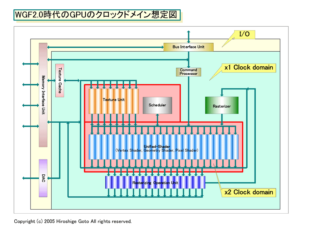
- Clock domain of the Shader core part is designated as 2 time speed
GPU this way, has loaded together the unit where character differs, so far being dragged to the fixed functional part, it was difficult to lift the clock. GPU remained always in operational frequency of 1 of several parts of CPU, parallelism was largely detached being high, at frequency. As for this, same even in the DirectX 9 being generation GPU, as for GPU extent it is distant in the GHz stand. As for this, with special care Shader, the fact that original efficiency cannot be shown is meant. For example, when it tries that GPU of 500MHz will achieve the same logical peak efficiency as Cell which can operate 8 SIMD processors with 4GHz, 64 Shader must be placed.
But, when it becomes WGF2.0 generation architecture, this problem reaches the point where it can solve partly. In WGF2.0 generation GPU, it is presumed that it collects Shader where many GPU vendors are the programmable operational core as コンピ…テーションコアアレイ. With mounting such as that, it is easy to separate Shader from other unit.
When it does, just Shader array separating clock domain, the question っ callous which is operated with the clock of 2 times that other unit becomes easy. For example, as for the whole GPU with also 600MHz operation, to operate with 1.2GHz it can do Shader array. It means that the operational efficiency of Shader rises rapidly.
Separation of such clock domain in the device of SOC type is done to popular. For example, as for the PSP tip/chip the CPU core is operational with time speed of other unit.
Of course, for that, Shader, from it is necessary to modify in the design which subdivides the pipeline. In addition, because as for accelerating with just the operational efficiency of Shader does not rise, as for other efficiency, when the bottleneck are other things, either entire efficiency does not rise. But, it reaches the point where operational efficiency with respect to theory can lift at least more easily. Whether or not time fast core appears in the first generation of WGF2.0 generation GPU, it is not understood, but GPU where Shader operates above 1GHz appears probably will be in the WGF2.0 generation.
The clock of GPU of WGF2.0 age
As for PDF editionthis
- In the possibility the design of GPU changing in the long term
When Shader operational efficiency rises, there is a possibility also the design philosophy of GPU changing. As for former GPU, in order to be able to increase efficiency with also the relatively low clock, it faced to the direction which increases the degree of parallel of processing. The quantity of Pixel Shader 4 -> increased at 8 -> 16 and many fold, GPU itself had enlarged because of that.
But, in the future, when we assume that most to be required with Shader efficiency, as for Shader efficiency itself can lift with time fast conversion of the core the inevitability which increases the quantity itself of Shader fades. For example, if even with same Shader quantity 12 as the mid range GPU of present condition, it operates with time speed, per 1 clock operation of 24 Shader minute becomes possible. Because of that, with GPU below mid range as for the spirit which increases parallelism there is also a possibility of becoming dull. Though, just the high end for efficiency demand for the ceiling not knowing, the possibility of keeping raising parallelism as still is high, but.
There is a possibility also approach itself of the design of GPU changing. The design period of present GPU at the half of CPU, from development start the product appears in the market in 18 - 24 months. Because with GPU, custom in the circuit design チ…ーン it does not do in acceleration that time is not required for the design. For example, David B. of NVIDIA Kirk (the デビッド B kirk) the person (Chief Scientist), you talked the reason as follows 3 years ago.
If チ…ーン it does "in the custom design, (GPU) as for more becoming high speed is certain. Problem is that time is required for the design. For example, after with CPU of Intel and the like, アーキテクチャデザイナ finishing work, also approximately 1 - 2 years spend time on transistor tuning. When the same thing it is GPU, in 2002, it means to put out TNT2 of 2GHz ",
In other words, with GPU addition of hardware specification and change of architecture are extremer than CPU. Because of that, when it is necessary to turn the design shortly in the cycle, so does, it is the case that for accelerating チ…ーン how you had not been able to have done in the custom design.
But, the technical trend of GPU is changing largely. New specification is not to add with the hardware, it actualizes with the software on Shader. Because of that, with flexible it has been about it will make Shader as much as possible in general purpose and to change. And, GPU efficiency is reaching the point where it depends on the acceleration of Shader. So when it does, if the architecture whose as for the GPU manufacturer is widely used in principle you spend time on the design, チ…ーン do in the high clock and you reach the point where it corresponds. Perhaps until recently it keeps changing to the development cycle which differs.
When that happens, like the CPU manufacturer high speed the processor core is designed and the development position which is accustomed, the possibility of embarking on GPU development comes out. Actually, in the past, the authorized personnel of a certain CPU vendor talked the idea such as that. If approach of the CPU design is introduced, because from high speed it is possible, to make GPU, you said that you have proposed to the parent company.
In addition, even with the next generation PlayStation, there was also a project of the GPU development which designates the Cell processor as the base. If Programable Shader is made in the SPE base and the luster riser and ポストシェーダ processing unit etc. are mounted with fixed function, that is the expectation which with that has become epoch-making GPU. In the future, more and more, there is a possibility seamless conversion of the design of such CPU and GPU advancing.
- The mounting Geometry Shader which designates the common hard conversion of Shader as prerequisite?
The WGF2.0 generation GPU where structure changes on the Shader center. As for this change, more drastic function, means the fact that the possibility of keeping being mounted in the form which is actualized with Shader is high. What it suggests that is Geometry Shader and "Tessellator (plane surface divided unit)".
Geometry Shader is the Shader stage which joins anew with WGF2.0. It has become the operation stage which ジオメトリシェーダ which handles the primitive (is also the times when it is called プリミティブシェーダ and) can send the program.
As for the difference with Vertex Shader which is in the same geometry pipe, as for Vertex Shader do the processing of the primitive unit. It tears the limit of former 1 apex input -> 1 apex output, it is possible to do the metamorphosis of the primitive. The fur to which was good and certain the ふ of the CG movie the ふ pointed it is the example which with ジオメトリシェーダプログラム of offline is formed in プロシージャル. That, even with the GPU hardware becomes possible.
The problem of Geometry Shader when it tries to mount this stage Vertex/Pixel Shader as the hardware which differs physically, is the point where mounted cost increases. When necessity it places Shader hard of the peak efficiency amount which is supposed, as Geometry Shader when it becomes, the several you must increase Shader hard. When programmable stage increases to the pipeline, in order for Shader of each stage not to become the bottleneck, more and more it becomes difficult to take balance.
Even now, Vertex Shader being ガラ empty depending upon application, Pixel Shader playing, there is a case such as reaching. If Geometry Shader joins, balancing becomes more and more difficult, the wastefulness of GPU furthermore increases.
But, if it mounts, Shader as Unified-Shader which is integrated even physically story changes. Because by the fact that logic Shader is allotted dynamically, it can take load balance automatically, it becomes easy to add Shader stage anew. GPU vendor side, balance without being troubled, it is possible to mount Geometry Shader. Because of that, the mounting to WGF2.0 of Geometry Shader is presumed that it is something which designates the integration of Shader hard side/general-purpose conversion as prerequisite.
- It makes Tessellator exclusive use hard, or actualizes with Shader?
Using Shader, it can actualize also Tessellator which does plane surface division, programmable. Actually, a certain information muscle has conveyed "the tessellation which is proposed at the time of DirectX 10, it was something which uses Shader", that. There was the stage of Tessellator even in the pipeline of WGF which last year is released, but there is a possibility of being the plan that this physically is mounted as Shader.
But, Tessellator of WGF which is was out this spring "GDC (Game Developers Conference)" in the presentation of Microsoft to last autumn. If we assume that it was something where Tessellator of originally WGF uses Shader this stops being the modification of hard itself. Tessellator stage going out, it does not mean that private hard is reduced, simply, it means that it has become the cancellation to allocate tessellation task to Shader.
The detailed circumstance where Tessellator was deleted from WGF2.0, it is not understood, but with another session of GDC, as for Microsoft it mounts Tessellation, as fixed functional hard, or it mounts still programmable as hard, or it suggested that it is argument. The advantage of fixed functional hard is high is that efficiency vis-a-vis mounted cost, but there is a problem where efficiency is restricted with the throughput of fixed functional Tessellator hard. Vis-a-vis that, if programmable hard, if Shader is used, the adjustment can do also tessellation efficiency unrestrictedly. But, if it actualizes with Shader, fixed functional unit compared to efficiency falls. In addition, Microsoft to standard pointed out also that it is not converted concerning programmable mounting.
It has been related this argument, to also the performance of Shader. Can, Shader with such as time fast conversion keep increasing efficiency inside GPU, if, it becomes easy to mount also Tessellator to Shader. In that case, the basic design of WGF2.0 generation GPU without changing, can actualize Shader based Tessellator with some modification. But, when it becomes an argument that, then sufficient efficiency you cannot obtain efficiency badly, it becomes a story that we want fixed functional hard after all. Perhaps, with that, objection being put, it is presumed that mounting the Tessellator stage to WGF2.0 went out.
In any case, the point of the case of Tessellator, with GPU, mounts still new specification, with fixed functional unit, or actualizes with programmable unit, or has shown the fact that it is argument. The seed of first trouble perhaps at this point in time is for programmable GPU which aims toward the graphic processor which can do also general-purpose processing. It is possible, if we would like to keep making programmable, but we would not like to drop either high efficiency as GPU. But, complicated processing, pursuing efficiency, when it can give with fixed functional unit, it does not cut the transistor in the resource which does not have general purpose to become necessary, general-purpose conversion ratio of altogether GPU falls. Trouble of the GPU vendor may continue still.
http://pc.watch.impress.co.jp/docs/2005/0502/kaigai176.htm