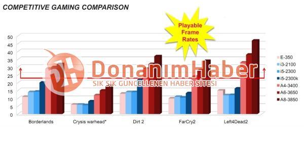
Llano IGP vs SNB IGP vs IVB IGP

Another 'leak'

55a.jpg


55b.jpg


TechPowerUp


If that's caccurate then I'm impressed!
 
they cherry-picked games and settings quite a bit, as an i3 2100 can totally destroy a E-350 sometimes. but that's pretty reasonable.

it's a no-brainer laptop chip!
 
Another 'leak'

If that's caccurate then I'm impressed!
Still looks like HD6450-ish performance. Well maybe a bit more for the faster parts. That's what everybody is expecting anyways, so I'm not really impressed. Still, great for a IGP, should make for quite nice not too expensive notebooks.
I'd be more impressed though if we wouldn't know the cpu part is unlikely to be competitive.
 
Is this suppose to be real?! First time I ever see those model numbers.

Yes, model numbers were known for some time now. Just search youtube for official AMD material regarding Llano ;)


@mczak

Bear in mind these are laptop chips with probably limited memory clock to just 1333MHz. I wonder how well it will perform with proper memory speeds e.g. 1833MHz+.
Besides extending that TDP range from 45W to 95W or maybe even 125W on desktop will give quite a big breathing room clock wise to this APU. Obviously GPU performance will be limited in most cases by memory bandwidth, but still it should be a lot faster than shown on these slides.
 
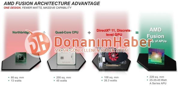
Could that mean that the A4-3400 is a 25W part, the A6-3650 is a 35W part and the A8-3850 is a 45W part? If so then this APUs would really be perfect for notebooks.

Again, this product codes and power consumption make no sense.

AMD demoed mobile A8-3510MX, which is prolly the fastets mobile part (45W TDP) against i7 2630QM.

So this are either desktop versions, but then the power consumption is not correct, or simply fake. The previously leaked model numbers for desktop Llanos were completely different.

Desktop:
Model Number CPU cores CPU Freq. L2 Cache Turbo Core Model GPU GPU Config GPU Freq. TDP Release Date
E2-3250 2 N/A 1 MB TBD HD 6370 160:??:? 443 MHz 65 W Q3 2011
A4-3350 N/A 2 MB N/A HD 6410 160:??:? 594 MHz 65 W July 20, 2011
A4-3360 N/A 2 MB N/A HD 6410 160:??:? N/A 65 W Q4 2011
A6-3450 4 N/A 4 MB N/A HD 6530 320:??:? 443 MHz 65 W June 20, 2011
A6-3450P N/A 4 MB N/A HD 6530 320:??:? 443 MHz 100 W June 20, 2011
A6-3460 N/A 4 MB N/A HD 6530 320:??:? N/A 65 W Q4 2011
A6-3460P N/A 4 MB N/A HD 6530 320:??:? N/A 100 W Q4 2011
A6-3550 N/A 4 MB N/A HD 6550 400:??:? 594 MHz 65 W June 20, 2011
A8-3550P N/A 4 MB N/A HD 6550 400:??:? 594 MHz 100 W June 20, 2011
A8-3560 N/A 4 MB N/A HD 6550 400:??:? N/A 65 W Q4 2011
A8-3560P N/A 4 MB N/A HD 6550 400:??:? N/A 100 W Q4 2011

Mobile:
Model Number CPU cores CPU Freq. L2 Cache Turbo Core Turbo Speed GPU Model GPU Config GPU Freq. MEM Freq. TDP Release Date
A8-3510MX 4 1.8 GHz 4 MB Yes 2.5GHz HD 6620M 480:24:8 500 - 725 MHz ? 45 W June 2011
A4-3330M 2 2.2 GHz 2 MB Yes ? HD 6480M 160:8:4 ? ? ? June 2011
? ? ? ? ? ? HD 6620Ga ? 400 - 500 MHz 667 - 800 MHz ? ?
? ? ? ? ? ? HD 6520Gb ? 400 - 440 MHz 667 - 800 MHz ? ?
? ? ? ? ? ? HD 6480Gc ? 400 - 500 MHz 667 - 800 MHz ? ?
? ? ? ? ? ? HD 6380Gd ? 400 - 500 MHz 667 - 667 MHz ? ?
 
maybe tipical amd/ati strategy to confuse everyone?

How on earth is that "typical"? They've had perhaps the most sensible naming strategy for years, only 6750/6770 and 6800-series are exception to the rule
 
I thought the picture said, "there are 25W-35W-45W series A APU. feel free to believe we're implying things, but technically we didn't tell you they are those from the other picture"
 
How on earth is that "typical"? They've had perhaps the most sensible naming strategy for years, only 6750/6770 and 6800-series are exception to the rule

amd/ati usually before a product launch does the possible to confuse intel/nvidia with astruse codename and changes of the product names
 
amd/ati usually before a product launch does the possible to confuse intel/nvidia with astruse codename and changes of the product names

Could you actually show some examples of this, too?
The Rxxx > Names was known long before the release, and SI/NI mess was confusing just as much inside AMD for what I've heard (and wasn't planned in the first place)
 
for example the simply fact that Rxx don't exist, instead we have a lot of unrelated name so that nvidia is hard at figuring what is what
then the Si/Ni confusion, from an interview it was a contingent plan but they used it to further confuse nvidia recicling codenames
then the famous wrong sp count
amd has a similar policy in which they show under nda a number of info and then one wrong or made so that they are able to almost know who broken the nda
this produce a number of rumors almost identical except for some ininfluential element

The new naming policy was known long before launch of HD5-series, true that they don't follow the old bigger number = better scheme.
The interview I've read said that the NI/SI confusion was never planned in the first place and caused too much in-house confusion too, NI was going to come first, but 32nm got cancelled > 40nm versions became SI, 28nm = new NI, but for them NI first makes more sense so 40nm = new NI, 28nm = SI.
Also, in case of NI, if my memory serves me right, the names are self explanatory - smalles island(s) name = slowest chip, biggest = fastest chip (or even card in case of Antilles), just the same logic as old Rxxx-naming.
 
It will be interesting to see how Llano boxes come equipped. Obviously this IGP is going to be very bandwidth limited. I can see now the notebooks with a single channel DDR3 interface completely crippling it.
 
So does AMD consider the entire chip an "APU?" Or just the GPU part?

Edit- It seems like the entire chip is an "APU." Which would mean the A6-3450, A4-3360 and A4-3350 are the 45w, 35w and 25w APUs respectively.
 
Last edited by a moderator:
Back
Top