ISSCC 2005

Deepak said:
So it looks like that PS3 will have 2PEs+16APUs with 512 GFlops, now if NV GPU could fill the rest then we can have 1TFlops. :)

No it will have 1 PE with 8 SPUs!

Its a huge chip, the shrink to 65nm will be purely to make it viable in a consumer market.
 
DeanoC said:
Deepak said:
So it looks like that PS3 will have 2PEs+16APUs with 512 GFlops, now if NV GPU could fill the rest then we can have 1TFlops. :)

No it will have 1 PE with 8 SPUs!

Its a huge chip, the shrink to 65nm will be purely to make it viable in a consumer market.
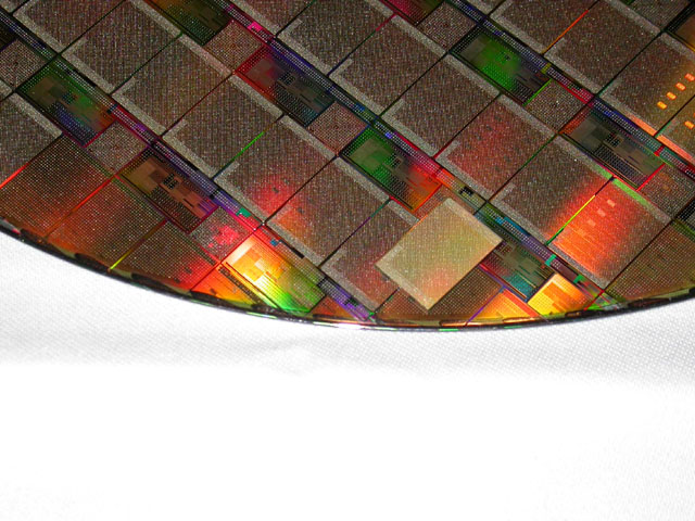
you look the wafer's picture
 
DeanoC said:
Deepak said:
So it looks like that PS3 will have 2PEs+16APUs with 512 GFlops, now if NV GPU could fill the rest then we can have 1TFlops. :)

No it will have 1 PE with 8 SPUs!

Its a huge chip, the shrink to 65nm will be purely to make it viable in a consumer market.

I agree it will be a 1+8 configuration, but it might be so for power consumption as well as size.

The original EE shipped with an area of 224 mm^2 and if they ship with the current chip area it would be already an improovement in yields: we are using 300 mm wafers compared to the smaller wafers used back in 2000.

Smaller chips, larger wafers = good ;).

A 65 nm CELL CPU with a 1+8 configuration should be quite nice and manufatcuring plant friendly given its relatively compact chip area and more constrained power consumption (compared to the 90 nm chip they presented now).
 
version said:
you look the wafer's picture

Yes, look:

kaigai008.jpg


And how I get it this are two PE, some EDRAM and something square shaped that I have no idea what it is, but I'm pretty sure this is not the GPU. ;)

Fredi
 
DeanoC said:
Deepak said:
So it looks like that PS3 will have 2PEs+16APUs with 512 GFlops, now if NV GPU could fill the rest then we can have 1TFlops. :)

No it will have 1 PE with 8 SPUs!

Its a huge chip, the shrink to 65nm will be purely to make it viable in a consumer market.
People seem to forget, that this $300 box is not just made of PEs .... there will be a GPU, some mem, a BlueRay drive, network interfaces, etc etc
 
DeanoC said:
Deepak said:
So it looks like that PS3 will have 2PEs+16APUs with 512 GFlops, now if NV GPU could fill the rest then we can have 1TFlops. :)

No it will have 1 PE with 8 SPUs!

Its a huge chip, the shrink to 65nm will be purely to make it viable in a consumer market.

So that means 256 GFlops for Cell, and how much for NV GPU? Will they both taken together cross 500 GFlops?
 
It would be more than 256 GFLOPS at 4 GHz, there is a VMX unit attached to the PU, this Vector Unit will not sit there twiddling its thumbs I'd think ;).
 
And what about PC scene when PS3 launches (2006). How much the then top of the line CPU+GPU combo will push?
 
Deepak said:
DeanoC said:
Deepak said:
So it looks like that PS3 will have 2PEs+16APUs with 512 GFlops, now if NV GPU could fill the rest then we can have 1TFlops. :)

No it will have 1 PE with 8 SPUs!

Its a huge chip, the shrink to 65nm will be purely to make it viable in a consumer market.

So that means 256 GFlops for Cell, and how much for NV GPU? Will they both taken together cross 500 GFlops?

Why does it matter if cpu/gpu combined is greater or less than 500GFLOPS???
 
Im lost with nm thing?
Isnt cell day one created with the hyped 65nm space and many many transistors in mind?
Why is possible at 90nm? Is there anything missing with this 90nm? Is this real cell chip?

is it they fit 65nm worth of transistors to 90nm? why people saying going 65nm is only for less heat less big more yield, like EE shrink? help!
 
In short, 90nm is "safe". 65nm would be great, but we'll have to see if Sony can get lots of 65nm chips by the time of release. If not, they can release at 90nm and then shrink it later on.
 
test circuit size equal about 250 million transistors
32 or 64 MB eDram
and 80 million transistors for logic that equal about 4 SPE , hmmm

im a stupid ?:)
 
one said:
psurge said:
This slide is confusing to me :
http://pc.watch.impress.co.jp/docs/2005/0208/kaigaip046.jpg

Does this mean 25.6 GB/s to memory and 76.8GB/s to other chips (GPU, etc...)?
It seems so.
A possible configuration in the PS3:
128MB XDR-DRAM @ 25.6 GB/s - CPU - (76.8GB/s FlexIO) - GPU - 128MB XDR-DRAM @ 25.6 GB/s

I think it has 50Gbyte/s for the mainmemory,not right?? Only 256MB
together,that is not a revolution that is a big shit(sorry),with this
we didn't see any CGI render and we didn't see the new Unreal Engine
in the same quality as the PC-version.To push all details in Unreal engine
you need 1Gbyte mainram( - winXP=900mb) and 256MB VRam(better 512MB),the story of HDTV in the nextgen are only a simply makeup,not
the same texturquality as in coming PC-graphiccards.And if it's true that
the PS3 coming out in the beginning of 2007 in Europe and Germany,
the Mark3D2007 Demo(PC) show us a better graphic than even PS3 game.You will see that......
 
Back
Top