DaveBaumann said:
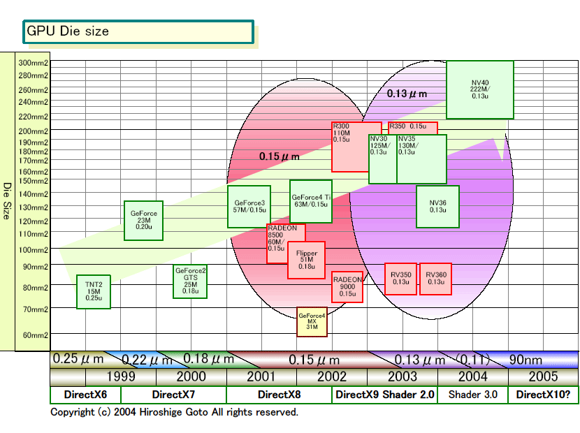
This is something Dave Orton pointed out to me the other day. Look at the low end chips - across the years the low end has stayed roughly the same die size (at the start, the low end is the high end as there was only one chip), the extra chips have been incrementally added at higher and higher die sizes.
The thing that really stands out is the die size difference between the NV36 and the RV350/360. nvidia must be taking a bloodbath in relation to ATI in the mid-range.
Also it would be really interesting to get a pricelist from TSMC to look at the cost differencial between the .15 and .13 processes. It doesn't look like ATI took much of a hit on die size for the .15u process and if the cost differential was in the range of 10% or greater for the process, they likely come out ahead on margins.
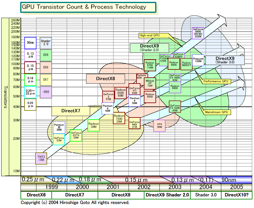
It also looks like ATI is has a much better physical design flow than nvidia, comparing the public die sizes and transistor counts. We know that nvidia is a heavy synthesis user, I wonder how much synthesis vs CBD (cell based design) ATI is using and if they are doing any significant full custom work in addition. That or ATI's designers are much better at designing to the design flow constraints allowing the synthesis tools to produce a better output.
Rough calculations show that a .13u R3x0 would be in the range of 160-180 mm^2. Assume standard frequency scaling metrics, a .13u R3x0 should also run in the range of 500-550 Mhz without additional architectural rework to the design. A little architectural rework should be able to get another 10% or so in frequency which makes the rumors 600 Mhz max frequency very reasonable.
Hmm, and a die size of ~260 or possible less looks probable as well. Though cost will probably still be up 80-100% per die compared to R3x0. Assuming a 4K wafer cost they are probably looking at an untested raw die cost in the range of $10 vs ~$7 for the R3x0. Assuming 60%/75% yield, they are looking at ~$17 and ~$9 per die respectively. Test, package, and assembly will probably cost another ~$10 per die on average, so $27 and $19 respectively. Merchant price for the R3x0 is probably in the range of ~$50. I would assume that the merchant price would be roughly the same for the 420. So profit per part look to be $23 for R420 and $31 for R300. Or a 26% decrease in margin.
Then again, I've never been in the merchant chip markets so my estimates could be totally off.
Aaron Spink
speaking for myself inc