From Ps3 architecture to comparing PS3 RSX and PC G70

liolio

Aquoiboniste
Legend
Helleo every body, i'm a 29 years old newbie.
I'm no more a gamers but i'm still please to follow hardware news.
A little thanks to the mods, who keep the forum interessenting.
I 've read all the topic concerning PS3 and XBOX360.
I've hard time understanding some very techies post but i've gone my ways.
I think a lot of person wizer and with a LOT MORE knoledge than my seem to keep things in a kind of war numbers.
What I want is to forget numbers and make some assomptions on the way chips are implemented in PS3 architecture (sorry for english, i DO my best).
The facts:
1 cell
1 rsx
256 mb xdr
256 mb gdr
We know that the two main chip (don't consu=ider sb as a main chip) are able to adress data anywhere on the 2 memory polls.
Some of you seem to see memories transaction that way:
X ------- Cell -------- G
D | D
R -------- RSX -------- R

I think in reality it's a lot a more linear
For what i've understand the heart of the PS3 is nor CELL or the RSX bus the Rambus BUS technology. unified bus architecture?
I see the the things working that way:

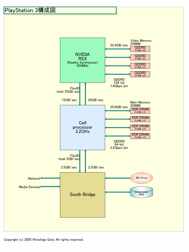
XDR-----XIO----EIB-----FlexIO----GDR
| | |
PPE PPE+PSE RSX
or CELL (based on linux devs articles)

EDIT( i can' t get a good spacing... so cell under XIO,EIB,FIO and RSX under FIO)
So my thinking is that the Ps3 is "architected" (really sorry for bad english) ALONG the Bus provide by RAMBus technology.
For ly it's teh only way the cell can access the gdr.
As an exemple the XBOX360 seem constructed AROUND the parent die.
So What?
Anybody seem concern with X4 and other we don't really know until more PR.
the main difference in G70 and RSX seems to be the implemention of some kind of FlexIO or weird memory controleur on the RSX.
So i want know what more knoledgeable than me think of my way understanding the PS3.
And if i'm not to wrong have them doing more guessing on RSx and PS3.
(NO FANBOYS)
 
liolio said:
XDR-----XIO----EIB-----FlexIO----GDR
| | |
PPE PPE+PSE RSX
or CELL (based on linux devs articles)

EDIT( i can' t get a good spacing... )
Wrap your example diagram in CODE tags...
Code:
XDR-----XIO----EIB-----FlexIO----GDR
               |          |             |
              PPE PPE+PSE        RSX  
             or     CELL (based on linux devs articles)
When I create such text diagrams I edit in MS Notepad with fixed space Courier, then copy and paste into the forum window.
 
The CELL architecture is an asymmetric multi-processor architecture. The concept of the EIB ring bus is the heart of how it communicates data. If you think of the EIB as a mini-ring topology network (hence the SoC), then the FlexIO is just another 'node' on that mini-ring network. As far as EIB is concerned, RSX might just as well be another CELL processor. It doesn't really matter. The FlexIO and EIB were designed for asymmetry.

PS3 is a NUMA system. This bring the notion of local memories and latencies and remote memories and latencies. It makes it harder for the programmer but it can make efficient use of available bandwidths. Some info on NUMA,

http://en.wikipedia.org/wiki/Non-Uniform_Memory_Access
http://lse.sourceforge.net/numa/faq/
 
Thank you Geezer

I see things more like this

................................... RSX...............................................................
.......................................|..................................................................
XDR---------XIO---EIB---FlexIO--------GDR3
.............................|...........................................................................
..........................CELL........................................................................

I agree with the statement of JAws.
I speak of a "weird" memory controler because it seems that rsx can be feed directly by cell or cell feeds the VRAM. And the same thing with the rsx can feeds the cell (seems not desirable from what i've already read) or sends datas to the Xdram.
Jaws the articles you have submit what very instrucive.
So the Xbox360 is a UMA or SMP(seems to be the same)?
But the memory controler is on the parent die(X360) do you think it was the best choise in regard of the small L2 shared with the three PPE?
 
In your pic, RSX accesses DDR through the FlexIO. I don't think this is the case. I though there was one connection to DDR direct, and another bus into Cell. I've never figured FlexIO tho'! Perhaps you're right, and that 78 GB/s is chopped up between different components, like a telephone exchange passing data through it?
 
I thought it was


xdr - xio- eib - xio - rsx - gdr over 2 64bit buses or perhaps it was 4 32bit buses ?
 
liolio said:
I see things more like this

................................... RSX...............................................................
.......................................|..................................................................
XDR---------XIO---EIB---FlexIO--------GDR3
.............................|...........................................................................
..........................CELL........................................................................

Yeah pretty much how I see it too....but I'm guessing an extra MMU looking after 'Turbo Cache' would sit in-between FlexIO and GDDR3,


....................................RSX...............................................................
.......................................|................................................................
....................................MMU (Turbo Cache)--------GDDR3
.......................................|................................................................
XDR---------XIO---EIB---FlexIO
.............................|...........................................................................
......L2 Cache (PPE) + 7x Local Store (SPEs)..........................................


The L2 cache of the PPE would likely be cache coherent with the 'Turbo Cache' too...


liolio said:
I agree with the statement of JAws.
I speak of a "weird" memory controler because it seems that rsx can be feed directly by cell or cell feeds the VRAM. And the same thing with the rsx can feeds the cell (seems not desirable from what i've already read) or sends datas to the Xdram.

Why do you say it's not desirable?

liolio said:
Jaws the articles you have submit what very instrucive.
So the Xbox360 is a UMA or SMP(seems to be the same)?

They usually go together but not the same. Xbox was UMA. The X360's not strictly UMA, because Xenos has local eDRAM.

liolio said:
But the memory controler is on the parent die(X360) do you think it was the best choise in regard of the small L2 shared with the three PPE?

There were rumors earlier in this year that XeCPU could be dual core. So depending on heat dissipation, more L2 cache with a higher clocked 'dual' core may have been a better option to 'boost' single threaded performance and less cache thrashing. But overall, I think the engineers have chosen the 'right' balance for their design goals with Xenos. I think they sacrificed the extra cache so that they could have the 'three' cores, one dedicated to geometry and one to physics with a 'master' core for general code etc...

They could've sacrificed the VMX units for more cache like the Gecko in Gamecube but it's obvious they wanted them for geometry, physics etc...so all things considered, the engineers made the best decision with the information available to them for a 90nm process. However, devs will always find something to 'bitch' about! :p
 
jvd said:
xdr - xio- eib - xio - rsx - gdr over 2 64bit buses or perhaps it was 4 32bit buses ?

xdr-xio: 4x16Bit
eib: 4x128 Bit-lanes in each direction
xio-rsx: FlexIO coherent link ??-Bit
rsx-gdr: 64Bit GDDR3
 
Npl said:
jvd said:
xdr - xio- eib - xio - rsx - gdr over 2 64bit buses or perhaps it was 4 32bit buses ?

xdr-xio: 4x16Bit

Agreed.

eib: 4x128 Bit-lanes in each direction

Agreed.

xio-rsx: FlexIO coherent link ??-Bit

RSX doesn't connect to XIO. RSX and CELL are connected with FlexIO inter-connects.

Including the SouthBridge, I suspect FlexIO is 64-128bit clocked 2.5-5 GHz, providing 40 GB/s R/W.

rsx-gdr: 64Bit GDDR3

The GDDR3 is 128bit bus, 700Mhz (1400MHz effective).

EDIT:

Shifty Geezer said:
In your pic, RSX accesses DDR through the FlexIO. I don't think this is the case. I though there was one connection to DDR direct, and another bus into Cell. I've never figured FlexIO tho'! Perhaps you're right, and that 78 GB/s is chopped up between different components, like a telephone exchange passing data through it?

You mean 48 GB/s like a cross-bar?
 
Jaws said:
Shifty Geezer said:
In your pic, RSX accesses DDR through the FlexIO. I don't think this is the case. I though there was one connection to DDR direct, and another bus into Cell. I've never figured FlexIO tho'! Perhaps you're right, and that 78 GB/s is chopped up between different components, like a telephone exchange passing data through it?

You mean 48 GB/s like a cross-bar?
I don't know what I mean :D I just remeber FlexIO had a very large bandwidth but I could never figure out what used it. Now I think it's a BW shared between attachments, where an 'attachment' is a GPU or another Cell say. But unlike an ordinary bus like to RAM, where one component can access all of the BW away from oter components, FlexIO is partitioned so each 'attachment' gets its own unshared BW.
 
http://pc.watch.impress.co.jp/docs/2005/0701/kaigai195.htm
kaigai_6a.gif
 
According to that picture, there's 40 odd GB/s FlexIO capacity not used. Presumably this is for multi Cell devices.
 
Code:
CELL + RSX Block:

................L2_Cache_[PPE]..................TurboCache_[RSX]
................|...............................|...............
................|...............................|...............
................+---<---+---<----FlexIO---->----+MMU............
................|EIB....|.......................|...............
................|4xRings|.......................|...............
....7x_LS-------+--->---+.......................GDDR3...........
....[SPEs]..............|.......................................
........................|.......................................
........................XDR.....................................

This maybe clearer. If L2 PPE cache and TurboCache on RSX are cache coherent (ccNUMA), it should help CELL and RSX address (read/write) to each others local memories more efficiently.
 
Here's a recent nVidia patent,

Patent said:
DETAILED DESCRIPTION OF THE INVENTION

Embodiments of the present invention provide memory management systems and methods for pixel data buffers in a graphics processing system using "copy-on-write" semantics. The display area is segmented into a number of tiles, where each tile includes one or more pixels, and pixel data for a particular tile is transferred from one location in memory to another only when the data is to be modified. To the extent that tiles are not modified during a frame interval, the need to transfer tile data between memory locations is reduced, thereby decreasing the demand for memory bandwidth.
...

Double-buffering of pixel data using copy-on-write semantics

This patent addresses several topics of recent discussion with PS3 and CELL + RSX. Namely, memory management, memory bandwidth reduction and tiling. These could be modifications/ customisations made to RSX that differ from the current G70/ 7800 PC card...

EDIT:

Cross-referenced nVidia patent,

Desktop compositor using copy-on-write semantics
 
liolio said:
So my thinking is that the Ps3 is "architected" (really sorry for bad english) ALONG the Bus provide by RAMBus technology.
It's a very interesting observation, as Cell's alias is Broadband Engine. Rambus is to host this year's Rambus Developers Forum Japan at July 7/8 and one of its keynote speakers is Masakazu Suzuoki, SCE Microprocessor Division, and the title is "Decision Process of CELL - Bandwidth dominates architecture". Apparently it's not too far fetched that PS3 is architected with a similar intention.

http://www.rambus.com/news/pressrelease.aspx?id=77
http://forum.rambus.co.jp/index.html
https://www.evt3.com/rambus/session.cgi
 
Here's a recent nVidia patent
What would be really interesting is if we were provided with the layout and size of these on-chip buffers, so I can actually force my rendering operations to be tile coherent where it counts.
Of course this is under assumption that the buffer size is not too tiny to be able to exploit effectively.

But I'm worried NVidia will turn a deaf ear to pleas for architectural details though, ruining much of the chances for using the architecture to its full potential :(
 
On-chip buffers? So there's local storage on a GPU in this patent for 'tiled' processing of a sort?

From Jaws' excerpt, I understand it that a screen (buffer) is segmented into areas and an area is only calculated when changed. In a static camera the background will remain the same so not be rendered. In 3D games usually the whole screen is in motion so I can't see any advantage.
But Faf is talking about something else with on-chip buffers.

Anyone care for a rough breakdown/translation of the patentese?
 
fafalada said:
But I'm worried NVidia will turn a deaf ear to pleas for architectural details though, ruining much of the chances for using the architecture to its full potential

You can always try to blackmail Jen-Hsun and Ken, with an x-rated 'Luna' demo! :p

Shifty Geezer said:
On-chip buffers? So there's local storage on a GPU in this patent for 'tiled' processing of a sort?

From Jaws' excerpt, I understand it that a screen (buffer) is segmented into areas and an area is only calculated when changed. In a static camera the background will remain the same so not be rendered. In 3D games usually the whole screen is in motion so I can't see any advantage.But Faf is talking about something else with on-chip buffers.

Anyone care for a rough breakdown/translation of the patentese?

Although the patent was describing double-buffering and frame-buffers, the concept is quite general.

Basically the patent implements logic that decouples 'buffers' from physical memory locations, tiles these 'buffers' and keeps them coherent in a tile 'table'. And the GPU doesn't have to be a tile based GPU.

So essentially you have these tiled 'logical' buffers mapped to 'physical' memory locations available anywhere in the system. And copy/write modifications to the tiled buffers can occur but the 'physical' memory is managed by this 'logic' so that memory bandwidth usage are minimised. The size's of the tiles can also be adjusted to match memory requirements.

This patent would be a good match for RSX + CELL in taking advantage of the NUMA architecture...
 
one said:
liolio said:
So my thinking is that the Ps3 is "architected" (really sorry for bad english) ALONG the Bus provide by RAMBus technology.
It's a very interesting observation, as Cell's alias is Broadband Engine. Rambus is to host this year's Rambus Developers Forum Japan at July 7/8 and one of its keynote speakers is Masakazu Suzuoki, SCE Microprocessor Division, and the title is "Decision Process of CELL - Bandwidth dominates architecture". Apparently it's not too far fetched that PS3 is architected with a similar intention.

http://www.rambus.com/news/pressrelease.aspx?id=77
http://forum.rambus.co.jp/index.html
https://www.evt3.com/rambus/session.cgi
Is anybody have news about that conference?
Google tell me nothing and I don't understand japenese.
another thing in the Unbalanced article by faout (lol) there something that hav hit me and for what i know seems reel.
The bandwith on X360 is 20Gb/s to parent and 20Gb from parent to Cpu.
So it looks like the ram can only be acessed at a rated of 20Gb/s shared between gpu and cpu.
Can anybody make that point clear?
But the main question is the rambus conference.
Thanks
 
Back
Top