[Beyond3D Article] Intel presentation reveals the future of the CPU-GPU war

http://www.theinquirer.net/default.aspx?article=37548

Hint #1 - Those chips pictured in the slides look REALLY familiar.
Hint #2 - x86 is an Intel strong point.

Rather than dither around about what you think Larrabee may or may not be, read the link.


-Charlie


I don't see any mention of how Larrabee handles coherence or caching in that story, but I did forget about the ring bus.

It sounds plausible that the large shared cache might exist as banks hanging off of the bus or a ring stop, each bank being more closely tied to one proceessor than it is the others.

To synthesize with the slides:

That would be consistent with the notion of non-uniform access.
Also, the mention of arbitrary data duplication (new instructions/cache line states?) could be part of a solution for excessive coherence traffic.

Since hits to cache do not generate coherency traffic, Intel would do well to implement controls on memory coherence, as well as provide avenues for minimizing common-case coherency broadcasts by allowing a fast way to bring chunks of data into multiple places in the shared cache.

The rest would likely be swallowed up by the huge bus width.


It sounds like an attempt to get a case closer to Cell's scalability, with an ad hoc "local store" that has coherency when needed, as opposed to the SPE's lack of it.

The persistence of private caches indicates there is a latency penalty to the large shared cache, something the threaded nature of the mini cores also seems to indicate.


That aside, as much as x86 is a strength in areas where it is already predominant, I do not think Intel could do all that badly if it didn't go fully x86 for Larrabee. (Look how well x86 has done in embedded, or cell phones, controllers, etc.)
On the other hand, if it wants to reuse the minicores as helpers in a future Core 4 or something, it might not be too painful.

As a GPGPU, I see Larrabee as being very competitive.
GPU, not so much, at least not for the near future. Perhaps Larrabee 2 or 3, if Nvidia and ATI decide to lay down and die.
 
The Article said:
So the question is, does the core support x86 instructions at all? If single-threaded performance is still roughly acceptable, it might make some sense for it to do so, and then you could think of the Vec16 FPU as an 'on-core' coprocessor that exploits VLIW extensions to the x86 instruction set. Or, the entire architecture might be VLIW with absolutely no trace of x86 in it. Obviously, this presentation doesn't give us a clear answer on the subject. And rumours out there might just be speculating on Larrabee being x86, so that doesn't tell us much either.
Groo The Wanderer said:
Hint #2 - x86 is an Intel strong point.
Thank you for confirming that.

Now, more seriously... Obviously, we read your article before. I don't think it clearly says "Larrabee is x86, that's what reliable sources are telling me explicitly, rather than me or my source presuming that based on the fact it's Intel, damnit!" - and it's not like it mattered much, anyway, and here's why.

The presentation points out the instruction set is VLIW, or at least has VLIW elements. If you add VLIW extensions to the x86 instruction set, it implies your Vec16 unit will just sit idle for 99% of x86 code. So, sure, you could run legacy x86 core on there. But who cares? It wouldn't even be any more per-mm2 efficient than traditional x86 cores then, even for highly multithreaded applications.

At best, they could disable the Vec16 FPUs to save power when they're not used, and pray to god it'd be half-competitive with Sun's Niagara/Niagara 2. Honestly, I doubt that, but who knows. I don't think it's the intended market at all anyway, but if they can create a single chip that is suitable for two market segments (or even more) rather than one, I'm sure they'd give it a shot.

And your article doesn't mention the existence of fixed-function units, which is an incredibly important point because it implies that Intel hopefully isn't naive enough to think that these cores are good enough on their own. I'm not sure how much you realise how slow a CPU or a GPU's shader core would be for things like texture addressing. It's just not a viable option. And that's necessary even for raytracing, in case that wasn't obvious. There is nothing magic about raytracing that makes fixed-function units obsolete.
 
As far as abstraction goes, why couldn't Intel design a chip that allows for both x86 instructions (that need to pass through a decoder) and native micro-op execution? Current 3D API's like DirectX and OpenGL aren't going away anytime soon. Developers don't access the metal directly, the software driver does. It'd be at the driver level that switches if an instruction stream passes through the decoder or not. Once past the decoder, instructions are put into a trace cache so they don't have to be decoded again much like the Pentium 4 did. Several x86 decoders could be thrown into the fixed function area and used as necessary by the actual cores. From a transistor budget stand point, the savings here are huge and allows scaling to a large number of cores/shaders while maintaining full x86 and GPU functionality.

In addition, there is no reason why the chip couldn't have a fully functional OoOE execution core. The x86 decoders are responsible for sending what instruction streams to what units for execution so they'd be the place to put branch detection logic. Native micro-op instruction streams have it even easier - they can bypass everything by indicating how branch heavy the instruction stream in some header information.

This design also allows for dynamic allocation of work between CPU and GPU style loads. This is great from an architectural stand point as one chip design can be made to scale from consumer to high end server chips. Manufacturing defects in the x86 decoders or the OoOE core would simply make it a consumer grade chip aimed at graphics.

The only downside is that necessity of large trace caches to keep things running smoothly and to keep the few x86 decoders from being over burdened. It'd likely be best to implement a small, nearly instant access L1 trace cache (< 3 cycles) and a larger, dedicated L2 trace cache (~10 cycles) per core. L1 data caches are dedicated per core but L2 data caches are shared throughout the entire chip. A large L3 cache (32 MB eDRAM, separate die) would act as both a frame buffer and shared unified cache. Code portability is one of the reasons Intel desperately needs to have x86 compatibility. However, the native micro-op design can change as long as it remains abstracted by various API's. Only the applications directly compiled for the native micro-op ISA would be of concern.

Another solution would to use some sort of code morphing software a la Transmeta instead of dedicated hardware decoders. With such a large number of core and even larger number of concurrently running threads, dedicating one thread to the purpose of code morphing an instruction stream for another thread isn't that big of a burden.

I think trace caches are not ideal for GPUs. They have inefficient instruction storage compared to a regular cache, because slightly different traces may be duplicated. They make sense when instruction fetch & decode are your limiting factors, but in a GPU/GPGPU/SIMD type of operation, this is not the case. You have a lot more data moving around than you have instructions. Also the trace cache helps with multiple branch predictions and fetching across cache line boundaries. GPUs do not have to worry about this because they have enough threads to just hide the latency in the case of a branch or other high latency instruction.

I don't think x86 as it is now is good for such an application. Even if you can use those microinstructions directly, they are not tuned for SIMD data sets. The uop to data ratio would still be very high, and it would be inefficient. In the end, you still need to have a x86 extension for GPU type applications. And in doing that, you might as well make them vliw-like instructions which can be decoded much more efficiently (possibly by specialized simple decoders). And if you want to do that, then you might as well just do away with the inefficient x86 stuff in the first place :p

OOOE also would be quite painful to combine with all this. It makes the entire chip much more complex (not just the decoders, you have to reorder instructions at retire stage etc), and again like the trace cache, it is really more useful for single threaded type applications where you want to maximize ILP.
 
I'm going to note (again) that if Intel added either fully vector or VLIW extensions to x86, it would be a bigger change to the ISA than the introduction of floating point.

VLIW especially would be a massive break from x86 semantics.

If it makes its way to becoming a full-fledged x86 extension, it would officially qualify as a Big Deal.

It would be a larger burden to have decoders for that and x86, though.
 
The problem is that there will always be parts of pretty much any application that's highly sequential. If you put in a great effort to parallelize your code you will probably still be left with a sizeable chunk that's not parallel. If you manage to parallelize 75% of your code, that remaining 25% sequential code means you won't see any performance improvements going beyond quad-core. There will probably be a market for say 16-core CPUs in the server space eventually, but for a PC I doubt it.


Depending on what exactly that remaining 25% of sequential code is doing it might not be much of an issue. It could be possible to use multiple threads to overlap and mask sequential code with other threads. Even taking that a step further I'm anxious to see how check-point based architectures perform through exploiting MLP and creating "cheap" locks.

How often is there going to be an application like you described which can't make use of those and other similar techniques? Now had you said time instead of code I think that could happen quite a bit with waiting on disk access or user input, and in which case the application is already too slow or (hopefully) isn't performance sensitive.
 
It could be possible to use multiple threads to overlap and mask sequential code with other threads.

If you can overlap it then it's parallel, so that code would obviously be part of the 75%. But there will always be code remaining that is impractical to parallelize.
 
In any case, you would need programs compiled for the new architecture to benefit. The VLIW interface is almost certainly meant to be able to target an individual core, with most of the rest of the bitmask being the micro-op. I expect branch and other hints there as well. They might even borrow from the ARM for that.

Otherwise, you're running in x86 compatibility mode, and any generic x86 CPU will beat it.
 
If you can overlap it then it's parallel, so that code would obviously be part of the 75%. But there will always be code remaining that is impractical to parallelize.


So yes, that would be most of the software that exists today.

I was arguing/hoping for a chicken-and-egg kind of scenario where future software attempts to solve problems on the desktop that couldn't have been done reasonably before because of the lack of cores. Hopefully they, like the computer vision I listed, will have the wonderful trait of being trivially parallel.

But like all things trying to predict the future of such a fast movie industry is difficult at best. :smile:
 
Well, I think back not too long ago, and I remember all the lengths gamers would go to in order to strip down their installs. I think it's not overly useful to get too hung up on how many cores a single app can use. Now, I'm not necessarily a fan of burning DVD's while you're playing a game, but it seems to me it is an awfully nice thing to have a general purpose install that works quite nicely for the most demanding applications (i.e. games) while still providing a rich set of always on services that you don't have to bang your head against the wall to fool around with/turn on/turn off just because you want to play your game now.

That doesn't mean there aren't useful limits, but if I were to seat of the pants it, I'd guess that multiply by 2 whatever you think a single app could usefully use to achieve that.
 
I think trace caches are not ideal for GPUs. They have inefficient instruction storage compared to a regular cache, because slightly different traces may be duplicated. They make sense when instruction fetch & decode are your limiting factors, but in a GPU/GPGPU/SIMD type of operation, this is not the case. You have a lot more data moving around than you have instructions. Also the trace cache helps with multiple branch predictions and fetching across cache line boundaries. GPUs do not have to worry about this because they have enough threads to just hide the latency in the case of a branch or other high latency instruction.

Having a shared decoder outside of the execution core easily makes fetch and decode a rather limiting factor. x86 decoders are large and complex part of the execution core. This design allows for something like 4 x86 decoders to be used with 16 hybrid CPU/GPU cores. Using trace cache allows for removing portion of the execution core so more cores can fit on a chip. Effectively you're bolting x86 functionality on to a GPU shader.

I proposed the separation of L2 cache into dedicated L2 instruction and a shared L2 data cache. That keeps the cores feed with a large pool of data quickly.

I don't think x86 as it is now is good for such an application. Even if you can use those microinstructions directly, they are not tuned for SIMD data sets. The uop to data ratio would still be very high, and it would be inefficient. In the end, you still need to have a x86 extension for GPU type applications. And in doing that, you might as well make them vliw-like instructions which can be decoded much more efficiently (possibly by specialized simple decoders). And if you want to do that, then you might as well just do away with the inefficient x86 stuff in the first place :p

It is true that the x86 ISA sucks. There have been many better architectures that have emerged and died through out computing history (Alpha anyone?) but x86 survived due to the necessity of software backwards compatibility and its early popularity.

OOOE also would be quite painful to combine with all this. It makes the entire chip much more complex (not just the decoders, you have to reorder instructions at retire stage etc), and again like the trace cache, it is really more useful for single threaded type applications where you want to maximize ILP.

The wonderful thing about starting an ISA from scratch is that you can incorporate various tricks to reduce the complexity of OoOE. For example, you actually put operation dependency information into the instruction stream as well as branch hints.
 
This thing is just a placeholder. Cell solves throughput, data-sharing, communication, on-die bandwidth, latency problems, whilst sitting between GPUs and CPUs on that "war" axis.

CELL is optimized for throughput.

It has absolutely pityful datasharing and communication latencies (SPU to SPU DMA latency is many times slower than even the slowest level 2 cache latency out there), on top of that coherence is software controlled.

This is what Intel adresses with caches, using a big shared fairly low latency cache to speed up synchronization primitives (atomic test-and-set) and inter-core buffers.

Cheers
 
I'm going to note (again) that if Intel added either fully vector or VLIW extensions to x86, it would be a bigger change to the ISA than the introduction of floating point.

I agree.

The justification for x86 boils down to: 1.) binary backwards compatibility and 2.) mature tool chain.

The entire presentation is focused on moving applications "to the left". This means the focus will be on new applications or new incarnations of old applications. So there is little incentive for ensuring backwards compatibility of old programs (which would run painfully slow on these cores anyway). New tools would also have to be developed to exploit data-level parallism of the new vector extensions.

One thing is the arcane encoding scheme, complicating decoder design, another is the condition flags that is written on most x86 instructions introducing false RAW hazards, which an in-order design would have a hard time negotiating.

All in all x86 compatibility would be a mill-stone around the neck of such an architecture, all IMO.

Cheers
 
Thank you for confirming that.

Now, more seriously... Obviously, we read your article before. I don't think it clearly says "Larrabee is x86, that's what reliable sources are telling me explicitly, rather than me or my source presuming that based on the fact it's Intel, damnit!" - and it's not like it mattered much, anyway, and here's why.

"What are those cores? They are not GPUs, they are x86 'mini-cores', basically small dumb in order cores with a staggeringly short pipeline. They also have four threads per core, so a total of 64 threads per "CGPU". To make this work as a GPU, you need instructions, vector instructions, so there is a hugely wide vector unit strapped on to it. The instruction set, an x86 extension for those paying attention, will have a lot of the functionality of a GPU."

:) Please note the terms used, I have been making blind guesses at future Intel products for a while, and occasionally hit the target. This might be one of them.

-Charlie
 
The possibility that was mentioned in that thread for breaking x86 semantics is also brought up again. These cores will most likely not be standard x86.

It's also a fine question as to whether these x86 cores would use SMT or some coarser threading model.

How ~64 threads on this chip compare to thousands on a GPU is another question.

edit:
The 64 number might only indicate the maximum number of threads that are in some kind of active or near-active state. A thread buffer of some kind could scale the thread count for relatively fast context switches that would increase the number of on-chip threads, since even GPUs don't really keep every single thread active.

That would be a change to how threading has been handled so far for x86.
 
Last edited by a moderator:
~2 years ago:

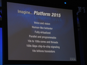
platform2015.jpg


http://www.intel.com/technology/magazine/computing/platform-2015-0305.htm


Platform 2015: Intel® Processor and Platform Evolution for the Next Decade

Overview: What's Over the Digital Horizon?
Without a doubt, computing has made great strides in recent years. But as much as it has advanced in the last 10 years, in the coming decade, the emergence and migration of new workloads and usage models to mainstream computing will put enormous demands on future computing platforms: demands for much higher performance, much lower power density and greatly expanded functionality.


Intel's CMP architectures provide a way to not only dramatically scale performance, but also to do so while minimizing power consumption and heat dissipation. Rather than relying on one big, power-hungry, heat-producing core, Intel's CMP chips need activate only those cores needed for a given function, while idle cores are powered down. This fine-grained control over processing resources enables the chip to use only as much power as is needed at any time.

Intel's CMP architectures will also provide the essential special-purpose performance and adaptability that future platforms will require. In addition to general-purpose cores, Intel's chips will include specialized cores for various classes of computation, such as graphics, speech recognition algorithms and communication-protocol processing. Moreover, Intel will design processors that allow dynamic reconfiguration of the cores, interconnects and caches to meet diverse and changing requirements.


Special-purpose hardware is an important ingredient of Intel's future processor and platform architectures. Past examples include floating point math, graphics processing and network packet processing. Over the next several years, Intel processors will incorporate dedicated hardware for a wide variety of tasks. Possible candidates include: critical function blocks of radios for wireless networking; 3D graphics rendering; digital signal processing; advanced image processing; speech and handwriting recognition; advanced security, reliability and management; XML and other Internet protocol processing; data mining; and natural language processing.


3. Large Memory Subsystems
As processors themselves move up the performance curve, memory access can become a main bottleneck. In order to keep many high-performing cores fed with large amounts of data, it is important to have a large quantity of memory on-chip and close to the cores. As we evolve our processors and platforms toward 2015, some Intel microprocessors will include on-chip memory subsystems. These may be in the gigabyte size range, replacing main memory in many types of computing devices. Caches will be reconfigurable, allowing portions of the caches to be dynamically allocated to various cores. Some caches may be dedicated to specific cores, shared by groups of cores, or shared globally by all cores, depending on the application needs. This flexible reconfigurability is needed to prevent the caches themselves from becoming a performance bottleneck, as multiple cores contend for cache access.


What will it take to realize this processor vision for 2015? Some major challenges loom, in both software and hardware. It should be mentioned that raw transistor count is not, in itself, likely to be a major hurdle for Intel. No other company has proven better at delivering to the goals of Moore's Law, and we can confidently predict that Intel processors will pack tens of billions of transistors on a 1-inch square die: enough to support the many cores, large caches and other previously described hardware over the next 10 years. There are, however, other challenges to be met.

1) Power and Thermal Management
Currently, every one percent improvement in processor performance brings a three percent increase in power consumption. This is because as transistors shrink and more are packed into smaller spaces, and as clock frequencies increase, the leakage current likewise increases, driving up heat and power inefficiency. If transistor density continues to increase at present rates without improvements in power management, by 2015 microprocessors will consume tens of thousands of watts per square centimeter.

To meet future requirements, we must cut the power density ratio dramatically. A number of techniques hold promise. As explained earlier, Intel CMP designs with tens or even hundreds of small, low-power cores, coupled with power-management intelligence, will be able to significantly reduce wasted power by allowing the processor to use only those resources that are needed at any time.


2) Parallelism
Taking advantage of Intel's future CMP architectures requires that tasks be highly parallelized—for example, decomposed into subtasks that can be processed concurrently on multiple cores. Today's single and multi-core processors are able to handle at most a few simultaneous threads. Future Intel CMP processors will be able to handle many threads—hundreds or even thousands in some cases. Some workloads can be parallelized to this degree fairly easily by developers, with some help from compilers, such that the processor and microkernel can support the necessary threading.

In image processing, for instance, the image can be subdivided into many separate areas, which can be manipulated independently and concurrently. Around 10 to 20 percent of prospective workloads fit into this category. A second group of workloads—around 60 percent—can be parallelized with some effort. These include some database applications, data mining, synthesizing, text and voice processing. A third group consists of workloads that are very difficult to parallelize: linear tasks in which each stage depends on the previous stage.


6) High Speed Interconnects
Intel's CMP architectures will circumvent the bottlenecks and inefficiencies common in other architectures, but may encounter new performance challenges. Chief among these is the communication overhead of shuttling data among the numerous cores, their caches and other processing elements. High-speed interconnects are therefore needed to move data rapidly and keep the processing from bogging down. Intel's approaches include improved copper interconnects, and ultimately optical interconnects (which move data at light speed).

The challenge lies not only in the interconnect material, but also the interconnect architecture. Ring-type architectures are being applied successfully in designs of up to 8 to 16 cores. Beyond that, new interconnect architectures capable of supporting hundreds of cores will be needed. Such mechanisms will have to be reconfigurable to handle a variety of changing processing requirements and core configurations. Interconnect architecture is an area of active and extensive research at Intel, at universities and elsewhere in the technology industry.
 
What do you mean by logically equivalent?
To be honest I fail to see this stuff sharing a lot in common with CELL.

I don't see it either. This looks more like the CPU in X360 but with more cores/cache. CELL is much different with a Master/Slave configuration and non coherent LS.
 
I don't see it either. This looks more like the CPU in X360 but with more cores/cache. CELL is much different with a Master/Slave configuration and non coherent LS.
these mini-cores look tinnier than the xcpu :
@90nm a xcpu is ~40m² it would be ~20mm² @45nm
probably less registers and a way shorter pipeline.

how does this hypothetical gpu compare in size to a G80?
 
Hopefully not old ... Intel talked a little about Larrabee at the Spring Developers Conference in Beijing:

Because official information on Larrabee is so sparse, I'm going to reproduce Intel's text from the press document and let those interested in the topic pick it apart:

Project Larrabee — Intel has begun planning products based on a highly parallel, IA-based programmable architecture codenamed "Larrabee." It will be easily programmable using many existing software tools, and designed to scale to trillions of floating point operations per second (Teraflops) of performance. The Larrabee architecture will include enhancements to accelerate applications such as scientific computing, recognition, mining, synthesis, visualization, financial analytics and health applications.

http://arstechnica.com/news.ars/pos...ially-owns-up-to-gpu-plans-with-larrabee.html

So it is x86-based.
 
Back
Top