ATI Technologies Interview: The Power of the Xbox 360 GPU

scificube said:
SI didn't know that shaders could use any instruction from the ISA with Xenos. I asked before on this forum and was told X360 devs would still have to use vertex and pixel shaders...but if those shaders can use any instruction then aren't shaders unified at the software level? Or is it more like...a pixel op can now be used with vertex data and visa-versa and there are still distinct shader types? The latter sounds more powerful to me but maybe isn't a flexible as the former. Any thoughts on this? Seem an interesting topic to me. I wonder what the possibilities are.

The vertex and pixel shader programs have access to the same instruction set. They're still seperate programs from a software perspective, though.
 
scificube said:
Still there seems to be something interesting in what was said...

I didn't know that shaders could use any instruction from the ISA with Xenos. I asked before on this forum and was told X360 devs would still have to use vertex and pixel shaders...but if those shaders can use any instruction then aren't shaders unified at the software level? Or is it more like...a pixel op can now be used with vertex data and visa-versa and there are still distinct shader types? The latter sounds more powerful to me but maybe isn't a flexible as the former. Any thoughts on this? Seem an interesting topic to me. I wonder what the possibilities are.


Xenos Article said:
Current graphics processor architectures can mark to "kill" a pixel in the pixel shader and this is the case with Xenos. However, as the architecture unifies the shaders the capabilities of both the shader program types (vertex and pixel) are available to each other, so the kill command will also operate for vertices. Although the vertex isn't retired in the ALU as it goes through the rest of the geometry pipeline to be set up vertices marked as killed will be ignored, effectively reducing the level of detail in the resultant geometry.


Q: Aren't the differences between PS and VS instruction sets quite small anyway?
 
scificube said:
It thought the link between Xenos and Xenon was 10.8Gb/s read/write not 24GB/s....what about the CPU having access to system memory...

I think it was a very confusing point. My understanding was that since Xenos is the memory controller, the normal read/write bandwiths between Xenon and Xenos and Xenos and memory were 2 different numbers 21.6Gb/s and 22.4Gb respectively
bandwidths.gif


I always thought the cache lock feature between the L2 and Xenos absorbed some portion of the 21.6Gb/s total bandwidth number. Now its appears that the cache lock feature has its own bandwidth of 24GB/s?:oops:

This has to be incorrect, I dont possibly see how it could be true because we have never seen/heard of any additional connections between Xenon and Xenos but we have heard of this "feature." If true its an incredible addition to the overall bandwidth of the system...

I guess on devs/Dave can validate this statement.
 
Last edited by a moderator:
That jumped otu at me to, but I didn't mention it for fear of looking dumb!

" The 22.4GB/sec link is the connection to main memory ...The GPU is also directly connected to the L2 cache of the CPUs – this is a 24GB/sec link Memory bandwidth is extremely important, "

This is news to me...
 
Alstrong said:
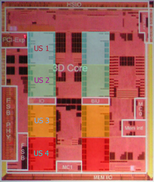
There was a die shot going around the forums awhile back.. can't seem to find it. It showed four rectangles in a column IIRC. Presumably, each is a shader array.
Prolly the die shot that I annotated:

b3d34.jpg


Alternative theories always welcome...

Jawed
 
blakjedi said:
This has to be incorrect, I dont possibly see how it could be true because we have never seen/heard of any additional connections between Xenon and Xenos but we have heard of this "feature." If true its an incredible addition to the overall bandwidth of the system...
The additional direct Xenos<>Xenon BW has been known about for a while. Jawed managed to thrash that out clearly! I don't think the size of the available BW was known though, or bidirectionality. 24 GB/s isn't too far off PS3's 35 GB/s CPU<>GPU. It is surprising more noise hasn't been made of this as it's more mindless numbers to add to the system bandwidth figures for the PR departments to extoll as virtues of their systems.
 
So Xenos has 22.4 GB link to main memory, a direct 24GB/s link to CPU, and a 32GB/s link to EDRAM which has 256GB/s internally?

Sound like it's got quite a bit of bandwidth overall to throw around.
 
scooby_dooby said:
So Xenos has 22.4 GB link to main memory, a direct 24GB/s link to CPU, and a 32GB/s link to EDRAM which has 256GB/s internally?

I believe that was his mistake. At least anywhere else it is referenced as 21.6GB/s (10.8GB/s both ways).
 
Not to mention the caveat that L2 cache access by XeCPU-Xenos is effectively only 10.8 GB/sec read, when accessing the GDDR3 at 22.4 GB/sec...
 
i dunno... it seesm as if he was saying that the 24Gb/s link was in addition to the 21.6 GB/s bidirectional link between Xenos and Xenon. 24Gb/s for cache lock as a completely separate function...

saying 21.6 (which is in their slides) and saying 24 is a big, non-subtle difference/mistake.
 
blakjedi said:
i dunno... it seesm as if he was saying that the 24Gb/s link was in addition to the 21.6 GB/s bidirectional link between Xenos and Xenon. 24Gb/s for cache lock as a completely separate function...

saying 21.6 (which is in their slides) and saying 24 is a big, non-subtle difference/mistake.

No, that's wishful thinking! We've been here before. I suggest you read the leak text + diagram from 2004, also the infamous recent 'leak' which even mentions it to be actually ~ 6 GB/sec...
 
Jaws said:
No, that's wishful thinking! We've been here before. I suggest you read the leak text + diagram from 2004, also the infamous recent 'leak' which even mentions it to be actually ~ 6 GB/sec...

I read those when they came out. I'm just going by the article which is .... recent. And we NEVER got an indication as to cache lock bandwidth before. I'm not sure whether Shifty was saying this guy was right or wrong...
 
blakjedi said:
I read those when they came out. I'm just going by the article which is .... recent. And we NEVER got an indication as to cache lock bandwidth before. I'm not sure whether Shifty was saying this guy was right or wrong...

Whatever about cache-lock, "effective" bandwidth, it's certainly going over the CPU-GPU bus. There's not a second bus there.

It's easy to make a mistake with a number like this, and it goes against the grain of everything else we've heard, so I wouldn't bet on him being correct and everyone else being incorrect.
 
blakjedi said:
I read those when they came out. I'm just going by the article which is .... recent. And we NEVER got an indication as to cache lock bandwidth before. I'm not sure whether Shifty was saying this guy was right or wrong...

10.8 GB/sec R/W CPU<->GPU 'IS' the cache locking bandwidth. This is another wishful thinking misinterpretation...
 
I dunno if the 24 GB/s figure is wrong, or they've improved upon it somehow, but the figure (10.8 x 2 or 24) is the XeCPU <> Xenos BW. There's no 24+21 GB/s! The cache locking is what enables direct throughput to this GPU BW, like a tap to divert data through another pipeline than just into the 'main tank'.
 
edit:

I typed this reply before lunch and then just submitted when I returned. I hope if I leave it it still has some value. If not. I'll remove it or the moderator can.

end edit:

I do need some clarification of that picture.

I see it two arrows between Xenos and the CPU. Why?

Between Xenos and main memory I see one arrow. Why?

I think that Xenos can consume all 22.4Gb/s writing to main memory or Xenos can do the same reading from main memory at that speed. 22.4Gb/s is what there to be used and Xenos can use it all up doing one or the other or a mix of both operations.

I don't think the two arrows in that diagram are insignificant. It makes sense to me that they represent the max read and write speeds of that link. Xenos cannot write or read faster than 10.8Gb/s. Xenos cannot send the CPU 21.6Gb/s of data nor take 21.6Gb/s from the CPU. The max is 10.8GB/s in one direction and in aggregate it's 21.6Gb/s if the max consumed in both directions simultaneously.

I think the reason 1 arrow labeled 10.8Gb/s wasn't used is because this would imply once you've consumed 10.8Gb/s there's no more bandwidth left which isn't true. It would only be true if you consumed that much bandwidth going in one direction....there's still 10.8Gb/s going the other way. Another reason it isn't used is that it looks bad compared to the link speed between Cell and RSX and muddying the water a bit may hide that.

I've always wondered how is it that IBM whipped up a solution that was nearly as fast as Flexio without the time and resources put into the effort like Rambus did. I don't think they actually accomplished that.

There was some developer's comments a while back that the X360 had some weird bandwidth limitations that was bothering them. Looking at Xenos and eDram I ruled that out and was left with them referring to the CPU having to share bandwidth to main memory with Xenos and this 10.8 Gb/s cap on transfer speed in one direction between Xenos and the CPU.

Perhaps the developer was referring to bandwidth needs related to procedural geometry/textures....10.8Gb/s seems good for post processing...err...I think.
 
Last edited by a moderator:
Your understanding matches mine. The 22.4GB/s is shown with one arrow because it's bi-directional, you can have an arbitrary split of reads/writes. The CPU-GPU bus is with two arrows to represent the fixed proportions. It's the same on PS3 (bidirectional bandwidth to GDDR3 and XDR, split busses between CPU and GPU, with 20GB/s going one way and 15GB/s the other).
 
Well I'm glad I'm not alone on that.

I just read the effective max is somewhere around 6Gb/s above. I don't know where that is from but I hope it's a little better than that or I misunderstand...because that's 45% off the theoretical max. What could possibly be causing do that!?!
 
Back
Top