AMD: Navi Speculation, Rumours and Discussion [2019-2020]

Status
Not open for further replies.
Rogame, who has good track record so far, claims it's 80 CUs for Big Navi

The table seems to imply bringing the RBE arrangement back in-line with the shader engine count, versus shader arrays in RDNA1. Other elements, like the geometry units and L1 caches were also arranged along those lines, so how that would be handled could be an area of change as well.

Wasn’t there a reference a little while back about RBE+? Something new?
:smile2:
I'm not sure I've seen the context around that term. I have seen driver references to RB+ modes, but those would be a much older concept than RDNA.

hum..... so 64 ROPs @ 2GHz = 1TB/s for FP16 writes or blending INT8 (8 bytes per pixel). Until GDDR6/HBM2, there wouldn't have been enough bandwidth to feed more fillrate anyway (@ Hawaii & Vega clocks on GDDR5/HBM1), compute needs aside.
Over the generations, the RBEs have been moved from direct links to the memory controllers to be clients of the L2, then L1, in addition to compression. The relatively modest debut of the DSBR included some indications of bandwidth savings as well.
There are optimizations for particle effects tuned to the tiny ROP caches that can lead to significant bandwidth amplification, and moving the RBEs inside larger cache hierarchies can give at least some additional bandwidth.

That depends on the packaging tech. If they use 2.5D TSV, SerDes is likely unnecessary since it can be dense enough to carry all the links as if they are on-chip 32B/64B data buses. Though having a read at the Zen 2 ISSCC presentation, there seem to be an argument against interposers (?).

Zen 2 CCD is 74 mm2, with the IFOP taking ~8% of the space, meaning ~6 mm^2. Each gives 32B read + 16B write per clock. Assuming one IFOP per two GDDR6 channels, that'd gives 8 IFOPs for ~48 mm^2, providing 384-768 GB/s aggregate at 1-2 GHz.
For clarity, is the first statement about not needing SerDes carrying over to the description of the IFOP link?
I thought IFOP still used SerDes, at 4x transfers per fabric clock.
I'm hazy on whether this figure includes the controllers along with the PHY blocks, which may change the per-link area. Whether a GPU subsystem with more thrash-prone caches would also prefer symmetric read/write bandwidth may also be an area adder.

In RDNA 1 they have reduced the L1-L2 fabric complexity from a 64/16 to 5/16. I had wondered why they even bother to have 16 servers for only 5 clients in the design. Now in retrospect, it looks like an incremental change over Vega towards this, given teasers like "X3D stacking".
The 16 seems to be inherent to the way the L2 slices serve as the coherence agents for the GPU's memory subsystem. A little less clear for RDNA/GCN is how the write path's complexity has changed. The RDNA L1 is listed as a read-only target, so how CU write clients are handled may add additional paths. One area I'm curious about is the RBEs and how their write traffic works the the L1, since AMD stated the RBEs were clients of the L1.

(late edit: One thing I forgot to add is that in the 5/16 arrangement, each L1 can make 4 requests per clock, so the L2's slice activity isn't limited by L1 count.)

One thing to evaluate at some point is what it has meant in the past that AMD's subsystem has maxed out at 16 texture channel caches, which are another term for the L2 slices. At least internal to the L2, per-clock bandwidth would seem to be constant between RDNA1 and RDNA2, barring a change in the L2 design. If the RBEs are L1 clients like they were in RDNA, what that means for L1 distribution in big Navi and the internal bandwidth situation could be interesting angles to investigate. A straightforward carry-over from RDNA1 would leave the metric of per-clock internal bandwidth the same across RDNA1 and RDNA2 implementations with 256-bit buses or wider.
 
Last edited:
For clarity, is the first statement about not needing SerDes carrying over to the description of the IFOP link?
I thought IFOP still used SerDes, at 4x transfers per fabric clock.
Yes.

I'm hazy on whether this figure includes the controllers along with the PHY blocks, which may change the per-link area.
The floorplan in AMD's Zen 2 ISSCC deck does not have separate desginations for IFOP PHY and controller. So presumably it means PHY and controller combined.

Whether a GPU subsystem with more thrash-prone caches would also prefer symmetric read/write bandwidth may also be an area adder.
It is true that GPU can have a vastly different access pattern that may require a different balance and/or provision for read-write traffic.

The 16 seems to be inherent to the way the L2 slices serve as the coherence agents for the GPU's memory subsystem.
I am not sure if it is inherent since the number of L2 slices have always been scaling alongside the number of memory channels. But in hindsight, it could be an overprovisioned, independent design parameter for parallelism in either the interconnect or the L2 cache itself, judging by the fact that Fiji has 32 HBM memory channels but still having only 16 L2 slices.

This perhaps indicates also that L2 cache is unlikely to go off chip, since it seems to have a role in enabling MLP not only in say the effective # of MSHR, but perhaps also lowering the probability of hotspot routes by overprovisioning the interconnect.

But it doesn't rule out another level of memory-side cache. :p

A little less clear for RDNA/GCN is how the write path's complexity has changed. The RDNA L1 is listed as a read-only target, so how CU write clients are handled may add additional paths. One area I'm curious about is the RBEs and how their write traffic works the the L1, since AMD stated the RBEs were clients of the L1.
L0 writing through to L2 did not change. L1 is no write allocate.
 
Last edited:
I am not sure if it is inherent since the number of L2 slices have always been scaling alongside the number of memory channels.
That's been an area where the higher end hasn't shown clear scaling.
From the _rogame table, the number of texture channel caches tops out at 16 for multiple GPUs.

AMD's RDNA whitepaper said 4 L2 slices per 64-bit memory controller, and the 4-stack HBM GPUs would have even more unsustainable crossbar dimensions if that constraint held.

For example, Fiji is indicated to have 16 in the following patch:
https://people.freedesktop.org/~agd5f/0001-drm-amdgpu-update-Fiji-s-tiling-mode-table.patch
There were some attempts at analyzing why a 4-stack HBM GPU showed areas of limited scaling over Hawaii, and one architectural corner may have been tests that may have isolated L2 bandwidth versus memory controller bandwidth.

L0 writing through to L2 did not change. L1 is no write allocate.
Is the claim that reads went to 16/5 from 16/64, but writes did not consolidate or did not need to consolidate?
 
That's been an area where the higher end hasn't shown clear scaling.
From the _rogame table, the number of texture channel caches tops out at 16 for multiple GPUs.

AMD's RDNA whitepaper said 4 L2 slices per 64-bit memory controller, and the 4-stack HBM GPUs would have even more unsustainable crossbar dimensions if that constraint held.

For example, Fiji is indicated to have 16 in the following patch:
https://people.freedesktop.org/~agd5f/0001-drm-amdgpu-update-Fiji-s-tiling-mode-table.patch
There were some attempts at analyzing why a 4-stack HBM GPU showed areas of limited scaling over Hawaii, and one architectural corner may have been tests that may have isolated L2 bandwidth versus memory controller bandwidth.


Is the claim that reads went to 16/5 from 16/64, but writes did not consolidate or did not need to consolidate?
Sigh, I figured I read the diagrams drastically wrong. The GL1 has 4 banks, and apparently the 4x 64B/clk L1-L2 figure applies to each GL1. It now makes perfect sense in how it simplifies the L1-L2 fabric design — it consolidates from one plane of 16/64 to four planes of 4/4 (persumbly interleaved by the same lower channel select bits used by the GL1 bank select).

Seems even more unlikely that any part of L1-L2 hierarchy goes off-chip then.
 
Last edited:
abHvXEjBo5CvTr8SpwsAdR-2048-80.jpg


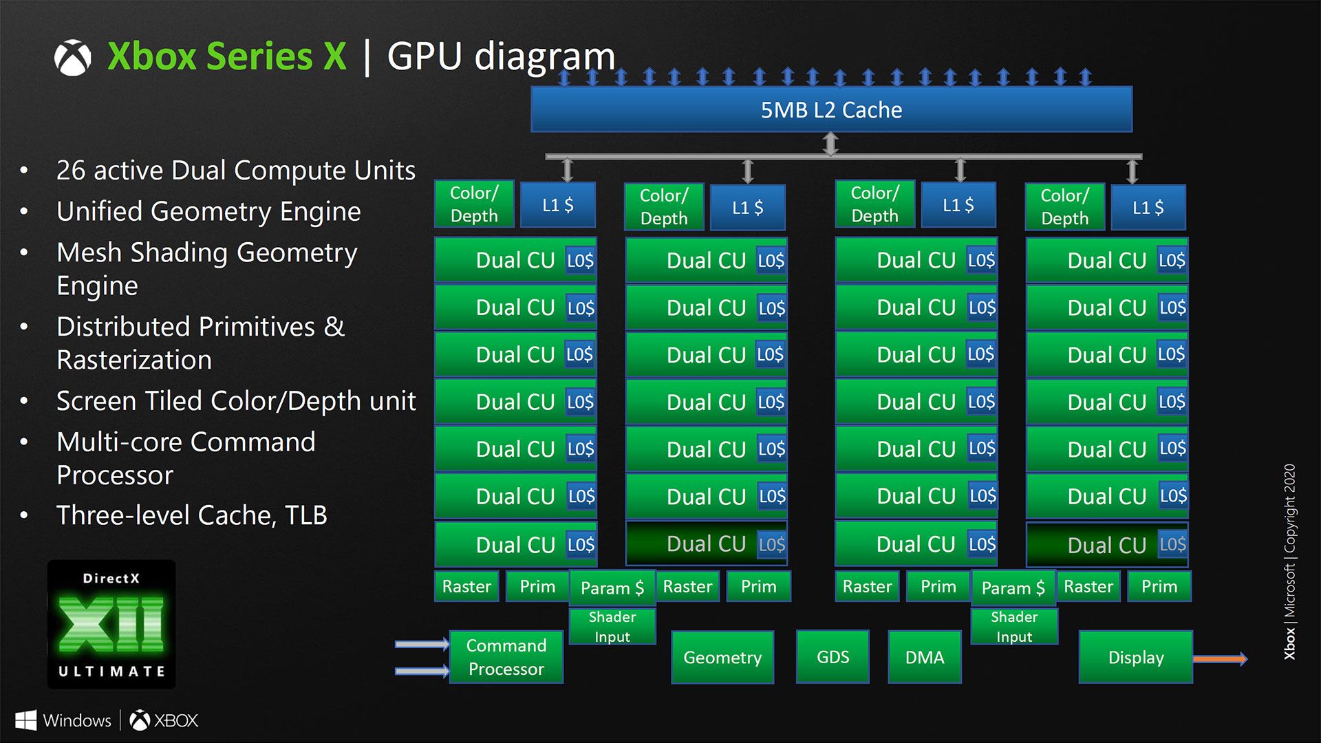
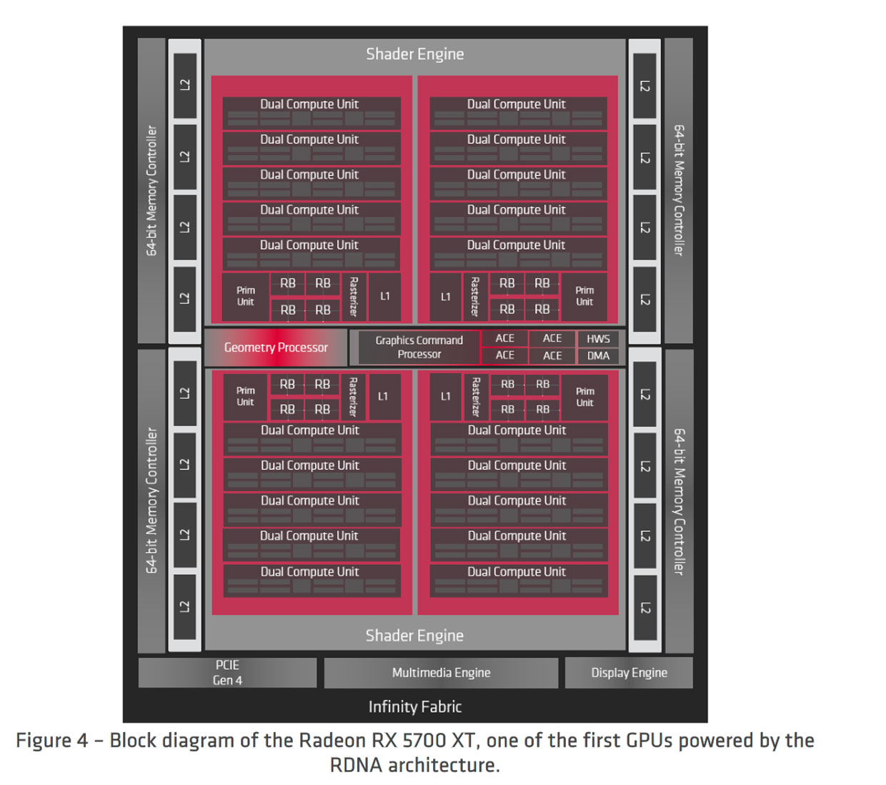
Looking at this, it looks pretty much the same as NAVI10 except there is more cache and more CUs. The shader engines are still the same structure. We can maybe assume RDNA2 cards to be very similar.
 
Maybe Microsoft will add ML resolution scaling to DirectX. Would be good to have something for it that is hardware agnostic at the API level. Since they are likely just using the shaders to do the inference without the use of tensor cores, it could probably work on any GPU, just depends on the performance they can get out of the hardware for inference while still running the game on the GPU.
 
Obviously most game engines will leverage DirectML because why not?

Maybe Microsoft will add ML resolution scaling to DirectX. Would be good to have something for it that is hardware agnostic at the API level. Since they are likely just using the shaders to do the inference without the use of tensor cores, it could probably work on any GPU, just depends on the performance they can get out of the hardware for inference while still running the game on the GPU.

I agree with both of you. Esp if we see it make it into games and is hardware agnostic. FidelityFX is not a bad option but DLSS is a much better option
 
Status
Not open for further replies.
Back
Top