AMD Kaveri APU features the Onion + bus like the PlayStation 4

onQ

Veteran
PS4 Liverpool APU & AMD Kaveri APU seem to have a few things in common.

Here is the Kaveri PDF. http://share.csdn.net/uploads/5232b691522ba/5232b691522ba.pdf


Kaveri+Onion+++.jpg


lvp2.jpg
 
I fail to see what's new or relevant to console forum.

Its interesting to see how close specific devices match the consoles and which paths the vendor that is providing the SoC's takes and why. I can't seem to load the file though, im getting 100 bytes a second.
 
Makes a lot of sense since the PS4 was originally planned with Steamroller cores rather than Jaguar cores. I would expect Kaveri to share many PS4 features.
 
Yes, reminds me of the PS4 GPU.

Does Sony have a OpenCL 2.0 library for that GPU ?

I am interested in the "System Integration" and "Architectural Integration" aspects of the new GPUs.
Even if the "System Integration" stuff may not be implemented in this iteration, I am curious to see if some of those benefits can be realized partially, or "manually" in other ways.
 
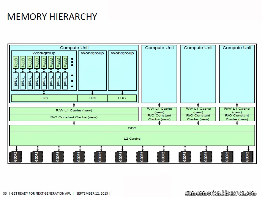
Is there a Kaveri APU coming out with GDDR5?

I wonder why it's showing GDDR5 in the Memory Hierarchy slide.

Kaveri+APU.jpg


APU+GDDR5+.jpg
 
Is there a Kaveri APU coming out with GDDR5?

I wonder why it's showing GDDR5 in the Memory Hierarchy slide.
The layout of the second picture looks a lot like a simplified discrete GPU diagram.
There is no mention of the CPU at all, so it may be a holdover from a GPU presentation.

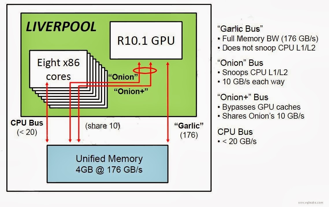
So only Onion+ bus (10 GB/s) is coherent in PS4's system memory?

It sounds like the CPU still can't snoop the GPU L2. Onion+ allows for pages defined to be coherent between host and device to skip this by never allowing data to sit in the GPU cache hierarchy. No explicit cache flushes are needed in that case, since the bus by design doesn't use them.
 
I'm guessing that the PS4 secondary chip is basically the same as the Bolton Controller Hub.

On a side note does anyone here know what the 'S' in SCH stand for? FCH is Fusion Controller Hub so I'm guessing the next generation of Fusion is something that starts with a 'S' but I haven't come across it yet.

Kaveri+APU.jpg


live0392-1361402893.jpg
 
On a side note does anyone here know what the 'S' in SCH stand for? FCH is Fusion Controller Hub so I'm guessing the next generation of Fusion is something that starts with a 'S' but I haven't come across it yet.
system or SoC would be my guess
 
Just to understand.

PS4 memory bandwith to CPU is 10GB/s Read and 10GB/s write?
And another 10GB/s shared?

It seems to me an incredibly low bandwith. Is it possible?
If confirmed this could be a big problem x developers.
 
I think the CPU <> DDR3 BUS is <20 GB/s bidirectional - you can read 20 GB/s, write 20 GB/s, or any mix of the two to a maximum 20 GB/s total read+write.
 
Isnt that still low?

4 core (8 thread) Haswell at 3.5 GHz (3.9 GHz turbo) is fine with 25.6 GB/s (and it shares that bandwidth with the HD 4600 IGP). Jaguar cores have around half the clocks and lower IPC compared to Haswell. Bandwidth shouldn't be a problem for them.

quote from another thread. Whilst it in regards to the other console with 30GB/s bandwidth its comparable imo.
 
Just to understand.

PS4 memory bandwith to CPU is 10GB/s Read and 10GB/s write?
And another 10GB/s shared?

It seems to me an incredibly low bandwith. Is it possible?
If confirmed this could be a big problem x developers.

Isnt that still low?


Low compared to what?

Seem like 20GB/s should be good enough for 8 Jaguar Cores especially now when data doesn't have to be copied over between the CPU & GPU.
 
Onion and Onion+ are described as different things because one is coherent and the other isn't, but they are the same physical bus?
 
I think the CPU <> DDR3 BUS is <20 GB/s bidirectional - you can read 20 GB/s, write 20 GB/s, or any mix of the two to a maximum 20 GB/s total read+write.

The slide it declares <20gb/s second bidirectional, but only 10gb/s for write and only 10gb/s x read.
It could be something similar to the X1 esram bandwith? (i.e. to have 20 gb/s you have to write and read at the same time?)

It seems low to me because if consider that this could be peak teoretical BW, PS4 will have just 7-8 gb/s for write and 7-8 gb/s x read to CPU.

Looking to hear something about from our forum experts!
 
quote from another thread. Whilst it in regards to the other console with 30GB/s bandwidth its comparable imo.

I believe that the other console you mentioned has 30 gb/s for coherent read/ write.
Non choerent should be more than twice that amount, 68 gb/s.
 
I doubt the CPU on XBox can read or write at a full 68GB/s, 30 seems reasonable, and I doubt that 20GB/s would be much of a constraint to the Jaguar cores.
The 10GB/s coherent write limit is more of an issue if the GPU is involved as it can be a real constraint on compute, but it only impacts GPU->CPU interaction, and there are other ways to get the same effect, notably, have the GPU write to garlic and DMA the results to Onion.
 
I believe that the other console you mentioned has 30 gb/s for coherent read/ write.
Non choerent should be more than twice that amount, 68 gb/s.

the only CPU link to the DRAM on the XBONE is the 30GB/s coherent link.

But that is off topic, as previously mentioned above the 20GB/s should be fine. I am interested in seeing what they can do with the 10GB/s coherent link, its a small amount but it seems nearly half the speed of the last gen consoles ram so its not that small.

The other option (flushing the compute lines of the cache) doesn't seem too bad with the modifications that Sony made to the cache architecture but it still something to be avoided I think.
 
Back
Top