Next Generation Hardware Speculation with a Technical Spin [pre E3 2019]

Status
Not open for further replies.
we have no reason to assume it will be monolithic, meaning the GPU could be it’s own chiplet.

a CPU chiplet makes a lot of sense for a launch system, especially if you go for a two tier setup.
And you don't need to lock down your CPU design with a branch from the mainline architecture that's two years old by the time the system launches.
Agree. Holiday 2020 (i.e. November) launch looks the earliest possible now, since Navi slipped to end of 2019 and this should give AMD enough time to perfect their 7 nm process.

I'd expect that a reasonably affordable package similar to Ryzen 3000, with:
1) a smaller dedicated memory IO die,
2) a 8-core Zen3 Milan die, and
3) one or two Navi dies delivering 10-12 TFLOPS in total​
should be perfectly possible by late 2019.

Maybe they could even manage to put HBM3 in that package, though this would be quite a stretch.

Given the price points we are working with I’m often baffled at the call for 10+ TF as being reasonable.
A console based on a SoC containing an AMD GPU has never had more than 1/2 the total TF capability of the top-end GPU from AMD at any time during this period.

This is due to the economics of using mid-range parts and techology to offset the costs of binning and packaging. And when they could pack several dies together or use a single integrated APU, this has always resulted in either much cheaper SKUs with the same or better specs, or significant performance gains for the same price.

The original Xbox, Xbox 360 and PS3 all used high-end GPU parts; and Xbox One X and PS4 Pro are arguably late attempts to repair performance issues of the original models under disguise of "4K" upscaling.

Newer features will define the generation not power output. Variable rate shading, mesh shaders/primitive, GPU side draw calls, RT, ML res, animation, physics and denoising.

Sure, but some of these improvements come with new pipeline stages (or a new API altogether), and this could require a costly redesign of the rendering engine - and maybe even a total revamp of artistic assets.

The latter is simply prohibitive for most game developers to undertake, as we've seen during similar technology transitions of the past.
 
Last edited:
It has too much baggage compared to a true gaming only design

We don't know much about Navi and the architectural improvements AMD has able to come up with it

I disagree. Vega includes a lot of useful new features which Navi would definitely use and expand on. For a start, HBCC virtual memory paging capabilities look especially promising in a game console.

Consider an IO die with a HBCC derived memory controller, and HBM3 die on the package in a high-end SKU. This configuration could give you:
* 4-8 GB of local HBM3 memory - 512 GByte/s;
* 8-16 GB of DDR5 system memory - 30-50 GByte/s;
* 30-60 GB of NVRAM scratchpad memory - 3-5 GByte/s.
All this memory would be connected directly to the crossbar memory/cache controller and mapped into virtual address space, with the ability to detect and unload idle pages from local memory to another partition.

That would be a cross between complicated high-speed memory subsystems of PS3 and Xbox One, but without the burden of manual memory management. Just load your assets all at once, and the OS will move them between memory partitions as necessary.
 
Last edited:
Holiday 2020 (i.e. November) launch looks the earliest possible now, since Navi slipped to end of 2019.

That is if there is Navi in there, i also think its Navi, but it seems abit late for Navi?

The original Xbox, Xbox 360 and PS3 all used high-end GPU parts; and Xbox One X and PS4 Pro is arguably a late attempt to repair performance issues of the original models under disguise of "4K" upscaling.

Agree on Xbox partly. For PS3 its abit more complicated then that, yes it used a high-end gpu, one from mid-2005 that is. OG Xbox used GF3 architecture for the most, with added vertex shader. Geforce 3 is a late 2000 product, didnt launch untill early 2001 due to stocked Geforce 2's. Geforce 3 was ready though, that would make the architecture allmost a year old by the time OG Xbox launched.

Only 360 which launched just some months after X1800, and some months before X1900.
Also, on 360 and PS3, OG Xbox, they werent APU designs like current gen?

Hard to say if this implys for mid gen consoles, but anyway
Pro and One X had much higher performance then their base variants, but nothing close to high-end GPUs at the time of their release. That would be what, Vega64/1080Ti for One X and Pro?

A mid-range Navi product with reasonable size, performance/watt ratio sounds realistic, although not as thrilling as a full fledge high-end gpu part. Also Tflops dont make or break a gpu either.
 
Something just crossed my mind, and I'd like some input. Some context:
  • This generation could probably go on longer than 2019/2020, thanks to the Pro and the X1X, but the base consoles would struggle to be AAA lead platforms for another 4-5 years. Unless they start facing situations like the Switch's 148x83 port of Ark.
  • The limiting factor of the base consoles is widely agreed to be their CPU's. They were the best option at the time, but still poor.
  • Console launches are expensive and risky.
So, my question is this: could the upcoming generation be designed to last longer?

I'll expand on this later, but right now, my dog really wants to play, and he keeps jumping on me with his squeaky toy, so I'm going to oblige.

Honestly don't remember when I quoted this post, but it's important to point out that Sony shows a dip in their FY2020 earnings with respect to 2018. This is largely assumed to be due to a console launch in 19 or 20.

Agree. Holiday 2020 (i.e. November) launch looks the earliest possible now, since Navi slipped to end of 2019. This would give AMD enough time to perfect their 7 nm process.

I'd expect that a reasonably affordable package similar to Ryzen 3000, with:
1) a smaller dedicated memory IO die,
2) a 8-core Zen3 Milan die, and
3) one or two Navi dies delivering 10-12 TFLOPS in total​
should be perfectly possible by that time.

Maybe they could even manage to put HBM3 in that package, though this would be quite a stretch.


This is due to the economics of using mid-range techology to offset the costs of binning and packaging. And when they could pack several dies together or use a single integrated APU, this has always resulted in either much cheaper SKUs with the same or better specs, or significant performance gains for the same price.

The original Xbox, Xbox 360 and PS3 all used high-end GPU parts; and Xbox One X and PS4 Pro are arguably late attempts to repair performance issues of the original models under disguise of "4K" upscaling.


Sure, but some of these improvements come with new pipeline stages (or a new API altogether), and this could require a thorough redesign of the endering engine - and maybe even a total revamp of all artistic assets.

The latter is especially problematic for game developers to afford, as we've seen during similar technology transitions of the past.

David Wang warned that multiple GPU chiplets would run into a crossfire situation where optimization is troublesome for developers. Perhaps if they pushed split frame rendering instead or tried to abstract it at the API level for devs in a console.

I disagree. Vega includes a lot of useful new features which Navi would definitely use and expand. For a start, HBCC virtual memory paging capabilities look especially promising for a game console.

Consider an IO die with a HBCC derived memory controller, and HBM3 die on the package in a high-end SKU. This configuration could give you:
* 4-8 GB of local HBM3 memory - 512 GByte/s;
* 8-16 GB of DDR5 system memory - 30-50 GByte/s;
* 30-60 GB of NVRAM scratchpad memory - 3-5 GByte/s.
All this memory would be connected directly to the crossbar memory/cache controller and mapped into virtual address space, with the ability to detect and unload idle pages from local memory to another partition.

That would be a cross between complicated high-speed memory subsystems of PS3 and Xbox One, but without the burden of manual memory management. Just load your assets all at once, and the OS will move them between memory partitions as necessary.

If they go this approach, I hope they would have two HBM3 stacks for a full 1TB/s bandwidth.

That is if there is Navi in there, i also think its Navi, but it seems abit late for Navi?


Agree on Xbox partly. For PS3 its abit more complicated then that, yes it used a high-end gpu, one from mid-2005 that is. OG Xbox used GF3 architecture for the most, with added vertex shader. Geforce 3 is a late 2000 product, didnt launch untill early 2001 due to stocked Geforce 2's. Geforce 3 was ready though, that would make the architecture allmost a year old by the time OG Xbox launched.

Only 360 which launched just some months after X1800, and some months before X1900.
Also, on 360 and PS3, OG Xbox, they werent APU designs like current gen?

Hard to say if this implys for mid gen consoles, but anyway
Pro and One X had much higher performance then their base variants, but nothing close to high-end GPUs at the time of their release. That would be what, Vega64/1080Ti for One X and Pro?

A mid-range Navi product with reasonable size, performance/watt ratio sounds realistic, although not as thrilling as a full fledge high-end gpu part. Also Tflops dont make or break a gpu either.

The chief reason consoles haven't been able to keep up is because high-end GPUs have had their TDPs grow astronomically over the last decade. How is a console supposed to compete with a 300W card?
 
The chief reason consoles haven't been able to keep up is because high-end GPUs have had their TDPs grow astronomically over the last decade. How is a console supposed to compete with a 300W card?

True, higher end components also are more expensive to produce i can think.
 
The original Xbox, Xbox 360 and PS3 all used high-end GPU parts

XGPU was 128 mm2, Xenon was 182mm2 and RSX was 186mm2. Times have changed. High end GPUs have gotten bigger and more power-hungry and console BoM budgets have not kept pace.
 
David Wang warned that multiple GPU chiplets would run into a crossfire situation where optimization is troublesome for developers. Perhaps if they pushed split frame rendering instead or tried to abstract it at the API level for devs in a console.
What if they weren't working on graphics? One rendering, one doing compute?

If they go this approach, I hope they would have two HBM3 stacks for a full 1TB/s bandwidth.
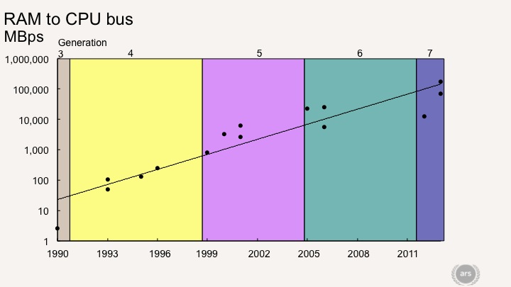
512 GB/s doesn't seem enough for a next-gen console to me. It's all of 3x PS4's BW. This Ars Technica article says RAM speed doubled per 1.5 years.

newrambus2.jpg


Though there's loads of variation around the trend. I wouldn't call it a line of best fit meself. Still, I'd be hoping for at least a 4x BW increase. Heck, that'd only match BW per pixel of this gen with nothing to spare for doing betterer stuff. 5x PS4 would be 880 GB/s.
 
Radeon VII offers allready 1TB/s bandwith? it shouldnt be a much of a problem for next gen consoles Navi then.
Are higher-end parts more expensive to produce?
 
Radeon VII offers allready 1TB/s bandwith? it shouldnt be a much of a problem for next gen consoles Navi then.
Are higher-end parts more expensive to produce?

Only HBM2 could reasonably offer that kind of bandwith and there is some question whether that could be produced in sufficient quantity to support console production volumes.

For comparison, the new Titan RTX is paired with 24GB of 14 Gb/s RAM on a 384-bit bus for 672 GB/s of total bandwidth.
 
Last edited:
What if they weren't working on graphics? One rendering, one doing compute?

512 GB/s doesn't seem enough for a next-gen console to me. It's all of 3x PS4's BW. This Ars Technica article says RAM speed doubled per 1.5 years.

newrambus2.jpg


Though there's loads of variation around the trend. I wouldn't call it a line of best fit meself. Still, I'd be hoping for at least a 4x BW increase. Heck, that'd only match BW per pixel of this gen with nothing to spare for doing betterer stuff. 5x PS4 would be 880 GB/s.

DCC partially mitigates the need for more memory bandwidth (relative to PS4), it's the reason PS4 Pro was able to get away with such a modest bandwith bump. It would make more sense to use Xbox One X's bandwith as your base and even that spec may have been more necessary for the additional capacity the extra memory chips provided instead of the bandwidth they added.
 
Last edited:
i also think its Navi, but it seems abit late for Navi?
Yes, the schedule looks tight.

Game console production has to commence one year prior to the scheduled launch. This would also typically coincide with formal public announcement and availability of developer kits.

So if Navi is the GPU for a November 2020 console launch, it needs to be available in volume by November 2019, with announcement and start of production by this Summer at the latest.

Maybe the initial console part will use a standard mid-range PC die, or a custom APU design, and an integrated multi-die package could be planned for a later refresh or a higher-end SKU.

If 'PS5 comes first' rumours are true, AMD could actually reserve significant production capacity for a later part of the cycle and serve the console launch in a tighter schedule.

But it's all really a stretch of imagination in absence of an official Navi anouncement.

I would just agree that a mid-range single-die GDDR6 part coming to replace Polaris by 2020 is a single obvious assumption at this time.

360 and PS3, OG Xbox, they werent APU designs like current gen?
Xbox and Xbox 360 use separate CPU and GPU chips, the latter also includes unified memory controller (and EDRAM cache in Xbox 360). However Xbox 360 S (Trinity) has an integrated APU-like chip, with CPU/GPU/EDRAM dies on a single package.

PS3 has two separate CPU/VPE (Cell/PPE, SPE) and GPU chips, each with their own memory subsystem, and also a separate SPE memory.

That would be what, Vega64/1080Ti for One X and Pro?
That would be 'enthusiast' level. 'High end' would be a lower-level GTX 1070 and R9 390X/Rx 480, or a potential Vega 48, i.e. 6-8 TFLOPS - just like the Xbox One X.

GCN and (N)CUs have the capabilities for it as architecture, but it needs more transistors than the (N)CU they use in most chips.
I'd think they provided for this capability during the principal development stage rather than postpone it to a potentially risky respin on a new node.
 
Last edited:
David Wang warned that multiple GPU chiplets would run into a crossfire situation where optimization is troublesome for developers. Perhaps if they pushed split frame rendering instead or tried to abstract it at the API level for devs in a console.
We've discussed this in the Navi rumours thread. There are recent NVidia research papers describing cache memory and thread scheduling optimisations required for a multi-die GPU which acts like one single unit to the developer.

AMD has an advantage of having working Infinity Fabric links to the central memory controller in both CPU and GPU dies.

The only - but significant - problem would be HBM interposer, which is very costly and incompatible with copper links used by regular processor dies.

What if they weren't working on graphics? One rendering, one doing compute?
512 GB/s doesn't seem enough for a next-gen console to me.
If they go this approach, I hope they would have two HBM3 stacks for a full 1TB/s bandwidth.
The HBM interposer problem has to be solved first. This may require stacking the HBM module on top of the memory controller (TSV), but there've been no announcements/ roadmaps for that solution so far.

Sure they can modify HBCC to work with GDDR6, but 1 TB/s would require 16-20 chips. I don't think it's currently possible at the price point.
 
Last edited:
DCC partially mitigates the need for more memory bandwidth (relative to PS4), it's the reason PS4 Pro was able to get away with such a modest bandwith bump. It would make more sense to use Xbox One X's bandwith as your base and even that spec may have been more necessary for the additional capacity the extra memory chips provided instead of the bandwidth they added.
mm... I wonder if there'd be a greater emphasis on GPU cache though what AMD plans for Navi is hard to say with nothing to go on, of course. xD Cache seems to be that much more important with RT added on top of things.

Polaris changed things up a tiny bit with the 3-CU groupings for sharing L1 (wiring/density optimization). Vega has their first iteration of ROPs being able to go through L2, but from what I gather, there are still some caveats about it (not sure if that's something nV had solved years ago already), but we should at least be looking at Gen2-ish (for AMD) for next-gen :?:

Hopefully we get a functioning DSBR - don't know if it was just a problem of general PC situation vs closed console development since 4Pro has the primitive discard accelerator (same thing I thought?). :???: Thought I recall some analysis that pointed to it not being at all like nV's tile-based work since Maxwell. (fuzzy memory)
 
We've discussed this in the Navi Rumours thrwad. There are recent NVidia research papers describing cache memory and thread scheduling optimisations required for a multi-die GPU which acts like one single unit to the developer.

AMD has an advantage of having working Infinity Fabric links to the central memory controller in both CPU and GPU dies.

The only - but significant - problem would be HBM interposer, which is very costly and incompatible with copper links used by regular processor dies.


The HBM interposer problem has to be solved first. This may require stacking the HBM module on top of the memory controller (TSV), but there've been no announcements/ roadmaps for that solution so far.

Sure they can modify HBCC to work with GDDR6, but 1 TB/s would require 16-20 chips. I don't think it's currently possible at the price point.
I’m not sure what you’re getting at with the interposer problems. Why would it be different than current Vega implementations?

As for GDDR6, I’d imagine they’d be content with less BW.
 
More food for thought: AMD's GPU development history

AMD's Top-end Single GPU Video Card
2012 - 7970 - 28nm - 3.79 TF
2013 - R9 290X - 28nm - 5.63 TF
2015 - Fury X - 28nm - 8.6 TF
2017 - Vega 64 (Air) @ Boost Clock - 14nm - 12.67 TF
2019 - Radeon VII @ Boost Clock - 7nm - 13.82 TF

Consoles based on AMD GPU
2013 - PS4 - 28nm -1.8 TF
2016 - PS4 Pro - 14nm - 4.2 TF
2017 - Xbox One X - 14nm - 6 TF

A console based on a SoC containing an AMD GPU has never had more than 1/2 the total TF capability of the top-end GPU from AMD at any time during this period. Keep that in mind when setting your expectations for the performance of next-gen consoles.

That’s grim.
 
I’m not sure what you’re getting at with the interposer problems. Why would it be different than current Vega implementations?
1) Cost of the solution - just Vega 20 GPU with 4 HBM2 exceeds the cost and power budget of the entire console by 1.5-2;

2) Packaging size - the space required for a massive central IO die (like the one in EPYC Rome) and even a single HBM3 module would not allow additional GPU dies with copper links on a typical package (like the one for Ryzen 3000); if we are using the interposer for all 5-6 dies - the costs raise again, see #1.
What’s to stop them from a Kaby Lake G type solution? The IO can all be on the GPU chiplet.
 
That’s grim.

It is grim and those numbers are a good grounding point for this situation. I do feel like they paint a little pessimistic scenario though. The increase in those numbers doesn't look that bad until the
Radeon 7. AMD has hit a pretty major power wall already with the Vega 64 pushing 300W and the process shrink to 7nm didn't bring them all that much on that similar Vega 20 design. However those chips have been pushed wayyy past their sweet spots due to the competitive landscape. Vega 56 gives over 10TF at 225W and people have been getting pretty good power savings on Vega 64 by sacrificing little bit of performance. I think there is reason to believe that a console chip could be closer to PC teraflops than before due to the hard power wall.

If you look at the Vega 64 review by Techpowerup, you can see that using a power save bios that limits the power draw to around 200W, they are still getting 92% of the performance.

https://www.techpowerup.com/reviews/AMD/Radeon_RX_Vega_64/29.html

https://www.techpowerup.com/reviews/AMD/Radeon_RX_Vega_64/31.html


Also Launch PS4 with 1.84TF on 28nm consumed around 140W, PS4 Pro consumes around the same watts on 16nm with 4.2TF and One X only increased this to around 170W with 6TF. That is great scaling with just one major node difference. Better AMD design with 7nm should make it easy(ish) to push past 10TF, even if the wall hits hard a little further. The base and possible premium SKUs throws a little wrench there, but at least the higher SKUs should get there.
 
Status
Not open for further replies.
Back
Top