PlayStation 4 (codename Orbis) technical hardware investigation (news and rumours)

Status
Not open for further replies.
The issue with just flipping bits in the page table to move data between the buses is I believe that it can end up requiring a GPU cache flush.
Since garlic is significantly faster than the coherent bus, copying the data might well be the faster solution depending how the data is used.
 
I'm not well-versed in the behaviors of page table modification, but a number of seemingly straightforward optimizations are either avoided or ruled out.
Having multiple pages mapped to the same physical address with different caching properties is one that at least x86 operating systems avoid, since having aliased pages with different properties can lead to undefined behaviors.
ARM indicates doing this on its processors leads to unpredictable behavior.

Changing the properties of a page wouldn't be enough to catch whethere there are other pages out there with unchanged properties, nor would it be obvious which processors currently have which aliases in their TLBs, or what number of accesses in various pipelines are running with which set of properties.
Messing with the cache settings for CPU-coherent memory could lead to accesses to the same address failing to update caches or main memory consistently, which breaks everything.

Other somewhat less momentous operations like migrating pages would require global stalls of everything or an architectural means of poisoning table entries so that invalid ones don't get used.
The massive number of queues, buffers, caches, and cores is such that for typically sized pages the delay in copying to a page with the desired properties is much less than what it takes to hang and flush the whole system.
There are scenarios in virtualized systems where page attributes need to be kept in sync between guest and host, and some cases require purging the TLBs or reverting to the most conservative attributes that maintain correctness.

I'm curious what Project Cars devs are copying from cached to uncached memory, and how much.
 
I'm curious what Project Cars devs are copying from cached to uncached memory, and how much.

Yep !

Not everything will need copying. For those buffers that the developers deem necessary to copy, there are also tactics and strategies to alleviate the impact. It all boils down to the applications. What exactly are they trying to achieve.
 
Could the mystery chip in the PS4 be a DPU?

What's a DPU?


http://www.cadence.com/ip/tensilica_ip/Pages/default.aspx

Tensilica IP Overview
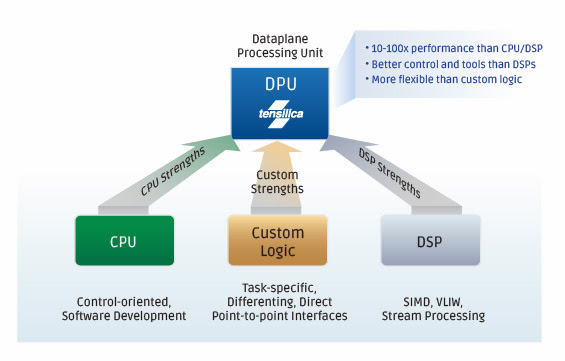
If your SoC design demands a highly efficient, programmable computational engine for a data-intensive task, you've come to the right place. The Tensilica® dataplane processing units (DPUs) combine the strength of CPUs, digital signal processors (DSPs), and custom logic with 10X to 100X the performance.

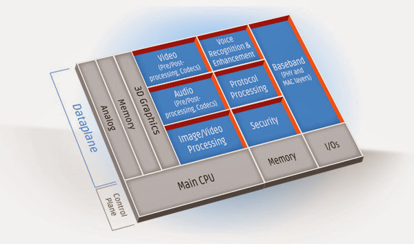
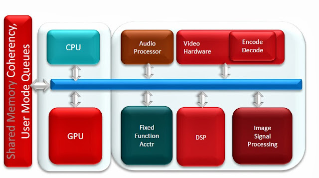
DPUs can handle BOTH performance-intensive DSP (audio, video, imaging, and baseband signal processing) and embedded RISC CPU processing functions (security, networking, and deeply embedded control).

The Tensilica processor architecture was designed, from the very start, to be easily modified to meet the demands of dataplane processing.

For some of the most common and broadly applicable tasks in the dataplane, we have ready-made solutions like our HiFi audio, voice, and speech DSPs, our ConnX communications DSPs, our IVP for imaging and video processing, and our Diamond Standard controllers for deeply embedded dataplane control.

For more specialized tasks, you can rapidly build your own customized DPU for tasks like image signal processing, video processing, security protocol processing, or network packet processing using our patented automated tools. The tools generate a complete matching software tool set, models, EDA scripts - everything you need to get into production quickly, at a fraction of the time it would take to design the function in RTL.


Slide from Sony's HSA Audio presentation showing a DPU.

http://www.slideshare.net/DevCentralAMD/mm-4085-laurentbetbeder

slide-3-1024.jpg


diagram-dataplane-n.jpg


dpu-new.jpg
 
"Mystery chip" is an awfully pretentious title to give something which in all likelihood amounts to misc/glue logic. But whatever floats your boat, Onq...
 
Sure. In fact, I bet the PS4 has four DPU's.


Notice how the CPU & GPU are together in it's own section then there is the audio ,video , image processor & other stuff off to it's own section just connected by the memory pipeline?

HSA+ARCHITECTURE++.jpg


The part that you see in blue is pretty much what you see sectioned off from the CPU/GPU which is what I'm guessing is the mystery chip. ACP?

diagram-dataplane-n.jpg
 
PLEASE, can you just stop with the wild guesses and completely baseless speculation? You have no actual evidence whatsoever that anything in your posts are even remotely accurate. Do you suffer from obsessive-compulsion disorder or something, just let the "mystery chip" remain a mystery, until the day (probably never) when some actual FACTS about it surface, okay?

Hunting for unrelated block diagrams on the internet of what the chip MAYBE PERHAPS is, is just a completely unproductive waste of time. Yours, AND ours.
 
"Mystery chip" is an awfully pretentious title to give something which in all likelihood amounts to misc/glue logic. But whatever floats your boat, Onq...
There's a chip on the motherboard that isn't understood. That makes it a mystery.

Hunting for unrelated block diagrams on the internet of what the chip MAYBE PERHAPS is, is just a completely unproductive waste of time. Yours, AND ours.
It's not possible for onQ to be responsible for wasting your time, as you are free to ignore his posts and go do something else. ;) I also don't consider it a waste of time in this thread as the topic is 'what hardware is in PS4' and this is a chip in PS4 which needs an explanation. That might be something mundane, but it still needs investigating. And it's not like there's any other popular line of discussion in this thread that's being interrupted. If someone enjoys investigating hardware possibilities, live and let live (until it becomes a cyclical argument or one that ignores the facts and generates noise).

His argument isn't even controversial. It doesn't claim 200 GFlops of uber power secret sauce. It's just suggesting that the ACP as described by Sony isn't inside the APU but is instead in a separate processor, that may be based on an Tensilica design.
 
PLEASE, can you just stop with the wild guesses and completely baseless speculation? You have no actual evidence whatsoever that anything in your posts are even remotely accurate. Do you suffer from obsessive-compulsion disorder or something, just let the "mystery chip" remain a mystery, until the day (probably never) when some actual FACTS about it surface, okay?

Hunting for unrelated block diagrams on the internet of what the chip MAYBE PERHAPS is, is just a completely unproductive waste of time. Yours, AND ours.

How is it baseless when the DPU is shown in the PS4 audio presentation & the Tensilica Audio DSP that's used in the PS4 is part of the DPU?

http://www.tensilica.com/products/audio
 
1) There's been some sound speculation (centered on IO). 2) If it was anything of substance, Sony would have talked about it, or it'd appear in the leaks. 3) A little general purpose coprocessor doesn't make sense in context of the system architecture where Sony could instead up the CPU clocks a bit, add cores, add GPU cores, etc. 4) A specialist coprocessor doesn't make sense because there's no knowing what the workloads will be, and Sony's emphasis has been on GPGPU and ease of development.

You'd be looking at something like a computation engine. If Sony wanted to do that, why not put in 4 SPEs on a chip? That'd be a great little chip, and also a PITA for developers who'd have to wrestle with another ISA.

Furthermore, the graph lists CPUs, not anything else. If the engine were more exotic I expect it'd use GPGPU too. So as it's not referencing system performance and instead CPU performance, this coprocessor would have to be a transparent CPU augmentation. And why stick that out in the middle of the board instead of inside the actual SOC?

At this point, there's no substantial evidence that the unknown chip is anything special, and discussion of the systems should assume it's something like an IO controller. Only in a rumour thread or PS4 hardware thread should the topic of the 'third' chip be covered.

DPU is the reconfigurable logic that I been reading about & seeing hints of from Sony over the last few years ACP is the name that we are seeing from Sony.

http://www.slideshare.net/DevCentralAMD/mm-4085-laurentbetbeder

Take a look at the slide & notice how they talk of the ACP in the same way that they speak of the CPU & GPU.


The ACP is not the Audio chip the audio chip is just a part of the ACP along with the image processor for the PlayStation Camera & some other functions. ACP is a DPU it has hardware accelerators & DSP's. This is exactly what Cerny was talking about when he said something about creating the hardware.
Remember me asking could Sony create fix function pipelines after the PS4 is released? it was because I picked up on what they was saying & I seen it over & over again so I knew it wasn't a mistake even when you all attacked me for saying so.


http://www.tensilica.com/learning-center/benefits-of-customization

Flexibility

Instead of a hard-wired block, you have a programmable processor-based solution, so you can make changes, even after tape out, via the software.

DPUs can be used instead of RTL blocks by adding the same datapath elements as implemented in RTL accelerator blocks. These datapath elements include deep pipelines, parallel execution units, task-specific state registers, and wide data buses to local and global memories. This allows DPUs to sustain the same high computational throughput and support the same data interfaces as RTL hardware accelerator blocks.

The big difference is in the control of the datapaths. With RTL, you freeze the control in the finite state machine (FSM). In a Tensilica DPU, the processor-based FSM is implemented in firmware, giving you maximum flexibility to add new features or make necessary adjustments.


Since you can create fixed function pipelines / hardware accelerators maybe there is a special DXT de-compressor that's making it easier for the PS4 CPU.
 
Last edited by a moderator:
onQ has come closer than anyone else on trying to figuring it out, and his post haven't gone "full retard" as compared to some others. So keep it up onQ... :smile:
 
Remember me asking could Sony create fix function pipelines after the PS4 is released? it was because I picked up on what they was saying & I seen it over & over again so I knew it wasn't a mistake even when you all attacked me for saying so.
Because the language you used and ideas you expressed were pretty much nonsense. You also talked of using the 64 command queues on the GPU to emulate fixed-function pipelines, which doesn't seem to have relevance to this discussion. The GPU queues are for the GPU scheduling and have nothing obviously to do with audio or custom processors that are realised on the motherboard - there's no point emulating fixed function hardware on the SoC with the ACEs if the actual hardware being emulated is on the motherboard.

I'm very happy for you to present ideas and explore possiblities, but do also recognise when you have been wrong (either materially wrong, or where you've expressed yourself unclearly and invited negative reactions against the ideas expressed as opposed to the idea you intended); you seem to come across quite often as suggesting your generally right even though everyone poo-poo's your ideas, and the reality isn't like that at all.

Since you can create fixed function pipelines / hardware accelerators maybe there is a special DXT de-compressor that's making it easier for the PS4 CPU.
Sony can put anything they want in that processor. Trying to determine its functionality from hypothetical uses and designs isn't going to get us very far. What's needed is either a paper-trail of design documents pointing to its function, which sadly are often open to interpretation, or some other explicitly evidence like a part number. I agree with the possibility of your theory that the extra processing blocks we know constitute PS4 could be housed in a discrete chip rather than on the SoC. I'm not yet convinced by your reasoning and evidence that it's a 'Tensilica DPU'. It could be (well, barring some info like number of pins on a Tensilica DPU being radically different to the count on the unknown chip), but there's little of substance by way of proof.
 
Because the language you used and ideas you expressed were pretty much nonsense. You also talked of using the 64 command queues on the GPU to emulate fixed-function pipelines, which doesn't seem to have relevance to this discussion. The GPU queues are for the GPU scheduling and have nothing obviously to do with audio or custom processors that are realised on the motherboard - there's no point emulating fixed function hardware on the SoC with the ACEs if the actual hardware being emulated is on the motherboard.

I'm very happy for you to present ideas and explore possiblities, but do also recognise when you have been wrong (either materially wrong, or where you've expressed yourself unclearly and invited negative reactions against the ideas expressed as opposed to the idea you intended); you seem to come across quite often as suggesting your generally right even though everyone poo-poo's your ideas, and the reality isn't like that at all.

Sony can put anything they want in that processor. Trying to determine its functionality from hypothetical uses and designs isn't going to get us very far. What's needed is either a paper-trail of design documents pointing to its function, which sadly are often open to interpretation, or some other explicitly evidence like a part number. I agree with the possibility of your theory that the extra processing blocks we know constitute PS4 could be housed in a discrete chip rather than on the SoC. I'm not yet convinced by your reasoning and evidence that it's a 'Tensilica DPU'. It could be (well, barring some info like number of pins on a Tensilica DPU being radically different to the count on the unknown chip), but there's little of substance by way of proof.


That was just me trying to figure it all out & how they was going to reprogram the hardware or whatever it was that the old CTO & Cerny was talking about in their interviews. I can't say for sure if the chip is a DPU but it matches up with the talk of programmable logic that I thought was a FPGA before & it's actually pictured in the slide from Sony's HSA Audio presentation.


The mystery chip might not be a DPU & the ACP could be a part of the APU with nothing to do with the mystery chip but everything that I have been trying to figure out about the reconfigurable hardware talk in the PS4 would be answered by the DPU.

Voice recognition,Voice Chat, Image Processing for the Camera & Video encoding/decoding all would be taking care of with the DPU.
 
Does Sony gain from keeping those stuff secret anymore, that all the consoles are rolled out?

I hope we have detailed hardware analysis documents like we had for the Xbox360. Maybe they are keeping some functionality under wraps before they make sure how much of that functionality will be used by the OS.

If it's implementation details, they can change it later.

Their developers seem pretty upbeat and confident about the deliverables in 2014. It should be pretty interesting to see what they are cooking.
 
Does Sony gain from keeping those stuff secret anymore, that all the consoles are rolled out?

I hope we have detailed hardware analysis documents like we had for the Xbox360. Maybe they are keeping some functionality under wraps before they make sure how much of that functionality will be used by the OS.

What does Sony gain from not telling us the OS reservations etc? It's not something that has to make sense... it's just that, a company secret.
 
What does Sony gain from not telling us the OS reservations etc? It's not something that has to make sense... it's just that, a company secret.

Whatever the case OS reservations seem to be one of the more closely guarded secrets of the consoles and will never be officially revealed. They weren't last gen. Too add to that veil of secrecy, they are somewhat dynamic, so any number that was accurate one day may not be accurate for long.

Hell the PS4 CPU clock isn't even officially revealed (unless I guess you count those DF post mortems).
 
Status
Not open for further replies.
Back
Top