Tegra 3 officially announced; in tablets by August, smartphones by Christmas

Exophase said:
Really? That sounds pretty farcical. "Sampling" should mean that you've actually sent samples outside the company. I'd expect it to be a step beyond having internally received first silicon.
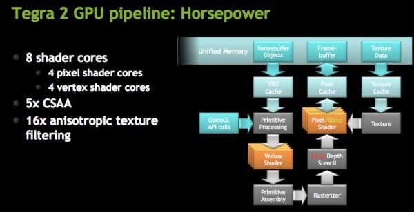
Yes, it's farcical. I've never seen sampling confused with tape out.

That said, it's not unusual to start sampling only days after first samples back from fab. I've seen it done after 2 days.
 
Are you sure? With a 5x performance bump

The 5x performance increase is for the entire SoC and that's including 2 more A9 CPU cores at a higher frequency compared to T2 ;)

and 12 shaders (unified or not) compared to T2's 8 shaders (4ps+4vs), it seems to me there's a pretty good chance the T3's shaders are hot-clocked.
The 50% more units (12 vs. 8) most likely should go to the pixel shader side. If Anand isn't wrong about the 4+4 in T2 then it'll go from 1 Vec4 PS to 2 Vec4 PS ALUs.

It's that or the whole GPU is clocked a lot faster than 300MHz.
Helloooo it's still on TSMC 40nm.

That or it's a completely new architecture, apart from the old APX2500.. Something closer to G98 arch without DX10 compliance?
Excuse me I'm just reading what Anand stated which obviously comes from the lion's mouth. If we're going to play the wild theories game before you're going into anything that will further increase die area/chip complexity you may want to again remember that it's on 40nm. Neither higher frequencies nor more die area are for free under the same manufacturing process.

Even if the market-BS 5x previous model performance translates into 2.5x real performance bump, increasing the ALUs by 50% would never be enough to hold that advantage. Unless nVidia has gone the Vivante way and has the whole Tegra 3 GPU clocked at ~900MHz.
Tegra 3 SoC = 5x Tegra 2 SoC. The 4*A9's might be clocked up to 1.5GHz in T3, put that against 2*A9@1GHz and a more modest increase from the GPU side.

How much faster did NV claim in the past T2 would be against T1 again?

Anand is just using the numbers presented in nVidia's own slides.
He's also stated 4 MADDs from the pixel shader units or the vertex shader units respectively. That's 8 FLOPs/clock from each side. There should be one more additional FLOP from the programmable blending unit in the PS ALU, but it's only available if the core isn't blending so it's rather silly to say 9+8, and what for anyway? You're not going to do anything GPGPU with merely FP20 precision either.
 
I'm sorry, i wasn't aware of any Tegra real numbers.. I assumed that the 8 cores where similar to the desktop architecture.

GPU_575px.jpg


So it's 1.92 Gigaflops.

http://www.engadget.com/2011/01/24/nvidia-tegra-3-equipped-with-1-5ghz-quad-core-madness-teased-b/

The performance chart is related to the entire SoC, not just the GPU part as i was thinking in the beginning. The 5x performance comes from 3x times the graphic power and 2.5x twice the cpu power.

So Kal-El has 4 Cortex A9-core and it's 40nm (right?)
Wayne may have 4 Cortex A15-cores and it's on 28nm.
From the time frame, i think Logan and Stark are on 20nm.. and probably based on ARMv8 architecture.

Finally someone that can decipher marketing hieroglyphs :)
 
Hm, so the GPU is now 12-core now instead of.. what, 8-core for Tegra 2? I never really got what that actually meant. I wish nVidia would talk in more discrete real life terms instead of just made up marketing terms. I wonder what this actually means though. That's only 1.5x the cores nVidia, how much better can it be ;p

It's clear from the Coremark scores that they have no problem pulling numbers straight from the website that were compiled with a much older version of GCC. It's good that they at least mentioned it on the slide, since it's such an obvious gotcha. One interesting thing is that all of the Tegra 2 Coremark submissions get about the same amount, while the Intel ones fluctuate quite a lot. Coremark scores are kind of hard to take seriously all around, but I guess that's not really going to change.

Are these the same cores as in Tegra 2 though ?
 

Okay, but nVidia claimed they were shipping samples in December 2010, not 12 days before February 16. So I think something doesn't add up here.

Same with the claim that competitors will only be sampling quad cores in 2012. I'm pretty sure the quad i.MX6 is going to be sampling long before then. Other vendors like TI and ST-Ericsson are, not entirely surprisingly, not as interested in quad core.
 
Last edited by a moderator:
Okay, but nVidia claimed they were shipping samples in December 2010, not 12 days before February 16. So I think something doesn't add up here.

Same with the claim that competitors will only be sampling quad cores in 2012. I'm pretty sure the quad i.MX6 is going to be sampling long before then. Other vendors like TI and ST-Ericsson are, not entirely surprisingly, not as interested in quad core.

A past leaked slide indicated that the smartphone AP30 SoC would have either a dual or quad core A9 option. If that should still be valid it would make sense for the smart-phone segment since quad core there could still be debatable today for its actual benefits. On contrary tablets can go to much higher resolutions than smart-phones and are a totally different chapter.

As for TI or ST (if you should be referring to OMAP5/NOVA9600) they're to arrive a LOT later than Tegra3. Besides there's also a difference between quad A9 and dual A15. On top of that OMAP5 strikes me as a MP4 GPU.

http://www.anandtech.com/show/4181/...-a9s-coming-to-smartphonestablets-this-year/4

Architecturally, Kal-El isn't a huge departure from what we currently have today with Tegra 2. If NVIDIA can increase clock speeds a bit we'll see better performance on lightly threaded workloads, but I'm not convinced of the gains to be had in single-tasking workloads from four cores in a smartphone/tablet. The bigger gains will likely come from any improvements to the memory controller as well as the faster GPU. This being said, NVIDIA does believe that even web page rendering can benefit significantly from a quad-core CPU so I could be very well proven wrong once devices are out in the wild.

These are all speculative opinions of course (especially the quote above); however I'm still not convinced that a higher concentration on the CPU side of things vs. a higher concentration on the GPU side of things could win in the long run. With 3D GUIs and the advent of some GPGPU functions in future SoC software I'd expect from the worldwide graphics leading IHV an exact opposite concentration.

It'll most likely come eventually, since I have severe doubts that if NV's roadmap has any merit that Logan will reach such a performance increase mostly from the CPU side. Rather the contrary and yes I might as well be wrong again here, but I don't see a gazillion of CPU cores at ultra-wild frequencies to make sense in a embedded SoC.
 
Really? That sounds pretty farcical. "Sampling" should mean that you've actually sent samples outside the company. I'd expect it to be a step beyond having internally received first silicon.

Well yes, it's farcical. It's also a way to get announcements out earlier.
 
metafor said:
Well yes, it's farcical. It's also a way to get announcements out earlier.
Other than for CPUs and GPUs (ever there often just rumors), the press hardly ever talks about when a chip has taped out.

So how do you know if people are making these false claims?
 
Other than for CPUs and GPUs (ever there often just rumors), the press hardly ever talks about when a chip has taped out.

So how do you know if people are making these false claims?

Let's just say I'm often surprised when I wake up and read a press release and think "wait, we've got silicon back already?"
 
metafor said:
Let's just say I'm often surprised when I wake up and read a press release and think "wait, we've got silicon back already?"
You must be working on very cool chips then. Good for you! ;)
 
I can't find any info on that. Arun in the other thread said that he was pretty sure about being 28nmLPG.

http://www.anandtech.com/show/4181/...-a9s-coming-to-smartphonestablets-this-year/2

The combination of the larger GPU and the four, larger A9 cores (MPE is not an insignificant impact on die area) results in an obviously larger SoC. NVIDIA measures the package of the AP30 (the smartphone version of Kal-El) at 14mm x 14mm. The die size is somewhere around 80mm^2, up from ~49mm^2 with Tegra 2.

http://www.xbitlabs.com/news/other/...8nm_Process_Tech_Not_Available_This_Year.html
 
From the Coremark webpage:
CPU Core Benchmarking

Although it doesn’t reflect how you would use a processor in a real application, sometimes it’s important to isolate the CPU’s core from the other elements of the processor and focus on one key element. For example, you might want to have the ability to ignore memory and I/O effects and focus primarily on the pipeline operation. This is CoreMark’s domain. CoreMark is capable of testing a processor’s basic pipeline structure, as well as the ability to test basic read/write operations, integer operations, and control operations.

Thats about real world performance.:rolleyes:
 
And here's source of T7200 score from slide - benchmark scores page. So it's not internal testing nvidia's result for T7200

Who cares if nVidia submitted the score or not? They still knew better. They COULD have ran a new fair score for T7200 and didn't. If they really didn't have access to a T7200 they could have at least ran theirs on the old compiler with the same flags. Or they could have just not made the comparison at all.

nVidia using a stock score is just a tactic to try to make it look legitimate. Besides, that score was submitted pretty recently and we don't know for sure that this company wasn't doing it on nVidia's behalf. In fact, why else would this company have submitted a score years obsolete just last November?

I wonder what else we can find on this Gerrit Slomma.

https://bugzilla.redhat.com/show_bug.cgi?id=491554 < reported a bug for an nVidia chipset
http://www.primegrid.com/forum_thread.php?id=1571 < released a CUDA prime solver

Okay, that probably doesn't say much on its own, except that he probably isn't anti-nVidia.

So what about ITS-Slomma, what do they do?

http://translate.google.com/translate?js=n&prev=_t&hl=en&ie=UTF-8&layout=2&eotf=1&sl=auto&tl=en&u=http%3A%2F%2Fwww.itsslomma.de%2Fabout.jsp

They're a small IT firm, I can't imagine why they would officially release a CoreMark processor score except on someone's behalf.

If nVidia really did ask for another entity to release this score for them then that makes things even worse.

Maybe someone should straight up ask him why he submitted the score.
 
Last edited by a moderator:
Back
Top