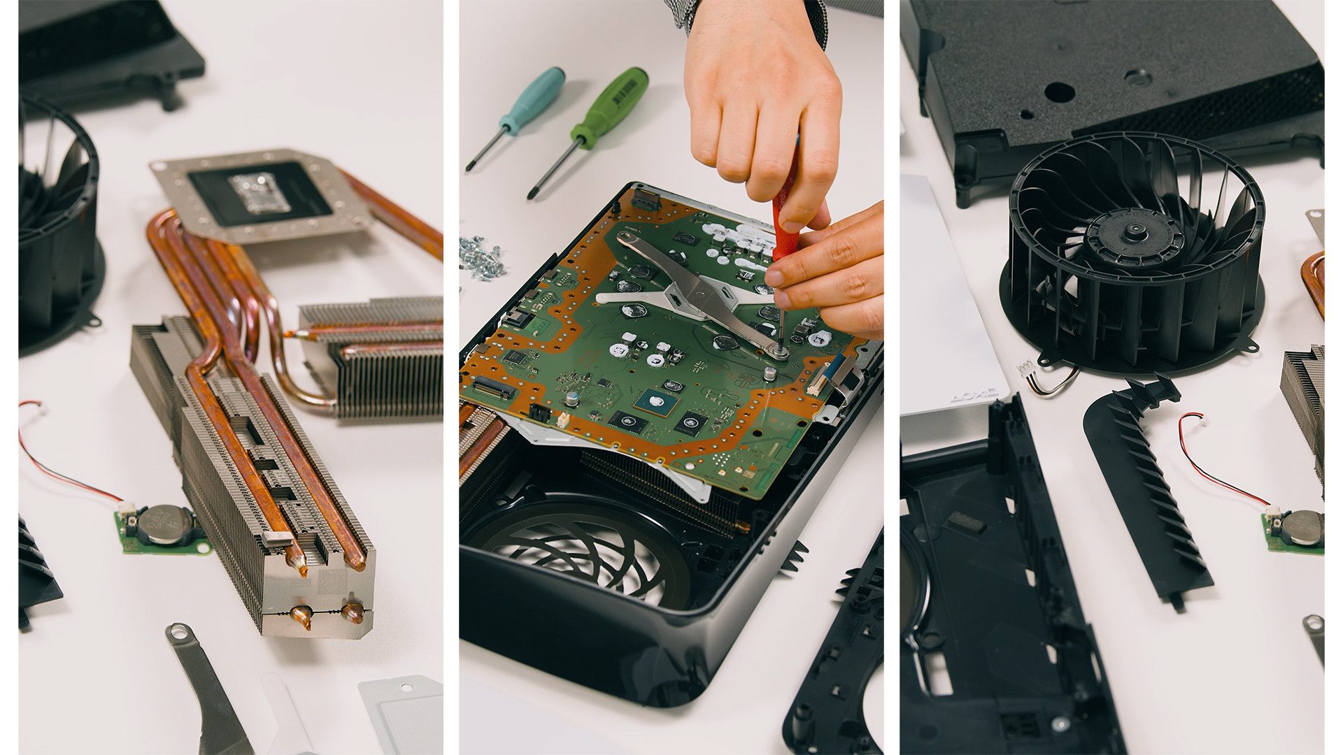
In all the videos that dismantle the PS5 Pro, do any of them list the chips with id's? Or rather does anybody identify the WiFi chip?
Not sure if anybody did say anything about the wifi chip, I did not follow this thread to closely , but I finally found the chip.
This video did not specifically mention the chip part number, but if you zoom in you can read it.
Which is J20H106, I googled it, but first hit was in a language I could not read, so I ran it through chatgpt.
Specifications
- Model Number: J20H106
- Equipment Type: Transmitter ReceiverFCC ID+1FCC ID+1
- Operating Frequency:
- Bluetooth: 2402 MHz to 2480 MHzFCC ID+1FCC ID+1
- Wireless LAN (2.4 GHz): 2412 MHz to 2462 MHzFCC ID+1FCC ID+1
- 5 GHz Bands:
- W52: Channels 36–48 (5180–5240 MHz)
- W53: Channels 52–64 (5260–5320 MHz)
- W56: Channels 100–144 (5500–5720 MHz)
- W58: Channels 149–165 (5745–5825 MHz)
- 6 GHz Bands (High Power Mode Only):
- U-NII-5: Channels 1–93 (5955–6415 MHz)
- U-NII-6: Channels 97–113 (6435–6515 MHz)
- U-NII-7: Channels 117–181 (6535–6855 MHz)
- U-NII-8: Channels 185–229 (6875–7095 MHz)
- Modulation Types:
- Bluetooth (BDR/EDR): GFSK, π/4 DQPSK, 8DPSKFCC ID
- Bluetooth LE: GFSK
- Wireless LAN: DBPSK, DQPSK, CCK, BPSK, QPSK, 16QAM, 64QAM, 256QAM, 1024QAM, 4096QAM
- Bandwidth:
- Channel Spacing:
- Antenna Gain:
- Bluetooth_1 (ANT3): 4.0 dBiFCC ID+3FCC ID+3FCC ID+3
- Bluetooth_2 (ANT4): 3.5 dBiFCC ID
- WLAN_2.4G_A (ANT1): 4.0 dBi
- WLAN_2.4G_B (ANT2): 4.0 dBi
- WLAN_5G_A (ANT1): 5.5 dBiFCC ID+1FCC ID+1
- WLAN_5G_B (ANT3): 5.0 dBi
- WLAN_6G_A (ANT1): 6.5 dBi
- WLAN_6G_B (ANT3): 6.8 dBi
- Antenna Type: PIFA/IFAFCC ID
- Antenna Connector Type: U.FL
So if its a 2x2 device then you can get a theoretical link rate of 2.5Gbps, Based on it being a 2x2 , 4096-QAM and 160Mhz bandwith., which is my guestimate.
Wether it supports MLO or not, I am not sure of.
Final post from me on the wifi chip, I promise
")
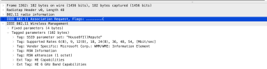
I had to do something for work and since the setup was done, I spent a minute in capturing the association request from the Ps5 Pro, sadly it does not support MLO (based on my curious glance at the traffic) with the current firmware I have on it. It might get it in a future fw update, but I am doubtful.
Looking at the pciture I attached, I expected to see a 802.11be MLO TAG.
Attachments
Last edited: