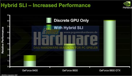
Nvidia's Hybrid SLI

Sure it is big, but it is an one-chip-solution and probadly include a GF8400-class-IGP, which will convince imo some OEMs. ;)
Sure, on second thought maybe RS780 isn't that much less expensive either:
- SB600: 35mm2
- RV610 on 55nm + 16x PCI Express 2.0 -> 60-80mm2?
- Extra costs related to having two packages, an extra bus, etc... (not huge but still)

NVIDIA probably has 90%+ yields on something like MCP78 too. If the GPU is defective, they sell it as a discrete chipset - and they also likely sell a version with redundancy in nearly every subsystem (fewer USB ports, fewer SATA ports, 100Mbit Ethernet instead of 1GBit, etc. etc.)

Even then, this makes me wonder how big G98 and MCP72 will be. I'd presume 85-90mm2 for the former and regarding the latter, it depends on what the differences with MCP78 really are... Also, I guess this means NV is going to keep competing in the lower-end IGP market with MCP61/MCP68 for some more time. Same for MCP73 in the Intel market once MCP79 comes out.
 
I suspect that the single-channel was not completely wrong, however. The most likely sources for such early leaks, AFAIK, are notebook manufacturers because the lead times are much longer there.

In the notebook arena, using one memory module instead of two can save power. And knowing NV, I'm sure they'd like to have some redundancy in the memory controller hardware to improve yields. So if you put 2 and 2 together, maybe there is some explanation for the previous rumour; although I'm quite skeptical it supports DDR3, but would be nice for notebooks if so.

The 'Performance' mode for Hybrid SLI is quite confusing. Of course, if what they're doing with Hybrid SLI and SLI 2.0 in general is much smarter than AFR, they might be able to disable most of the GPU but not absolutely all of it, and it'd still help performance. I'm very skeptical that's the case though...

P.S.: If MCP78 is already 125mm2, I wonder how big MCP79 will be with an extra dual-channel memory controller. Of course, it probably is on 55nm, but still!
 
Not impossible. That'd allow them to just keep the shader core on the 'IGP-less' 730i and still accelerate everything a little bit. Effectively, it would become 3DFX's Sage true successor! ;) Too bad it couldn't help for triangle setup too (or could it?)

This might be a decent plan redundancy-wise, as you already have half the shader core disabled for the MCP79-S, so the only case you can't handle is when the input assembler or both 8-wide SPs are unusable. Honestly, that's not even worth another bin.
 
A word to Fuad:
Confusing chipsets for Intel and AMD processors after you've seen a photo -and description of its abilities/supported CPU's- of the thing and its socket is just downright stupid...

At least Lars got it right the first time, he didn't even mix the wrong codenames like you did (MCP78 is AMD-only, just like 780a, and 780i is basically 680i + NF200 PCIe 2.0 bridge chip, as the 790i is a completely different beast with native PCIe 2.0 and DDR3 support, coming early next year). ;)
 
Last edited by a moderator:
That would be quite the IGP. Packing video capabilities/performance far superior to intel's, it also packs DX10 albeit not really usable though.

Actually, looking at the history of IGP development, I doubt Intel/Nvidia/ATI won't be really far from each other when Intel gets the basic things straightened out-like drivers. Current drivers in XP put the GMA X3000 around ATI X1250, and GMA X3500 will be out before next year, with GMA X4500 in Q2 of next year. Really being a Geforce 8400 is one thing, but being based off is another. X1250 is based off X700. It performs nowhere near it.

Intel is behind, but they are catching up rapidly. I doubt they'll exceed much if they do though, because its an IGP.

The X3500 will fix most of the things that lag the ATI/Nvidia IGP parts in video capability, with lots of the boards featuring support for HDMI and such. They also bring DX10/SM4.0 support in hardware, but not sure if there is really any performance advantage over the X3000. Still the biggest thing is drivers. Hope they get fixed by early next year.

On a site note, Japanese site PCWatch reported that the die size of G965 is 128mm2. So G965 isn't exactly tiny either.
 
X1250 is not 'based' on X700 in terms of specifications, only in terms of architecture. MCP78/MCP79 are literally G98, while RS790 is afaik literally RV620. There's a huge difference here. As for bandwidth - I wouldn't worry too much about that, since both could potentially have as much bandwidth as the 8500GT via HT3 or the MCP79 dual-channel memory controller...

And yes, G965 is on 90nm and about the same die size as MCP79 will be on 55nm (although the latter is single-chip and integrates the southbridge). However, the performance will be very different; X4500 vs MCP79 is the only interesting question here, and if Intel is claiming just 3x G33, then they won't stand a chance (but won't be incredibly far behind either). Also, power consumption will be interesting to compare, especially MCP73 already beats G33 on power efficiency and will have design wins based on that...

I obviously agree Intel is catching up rapidly - but let's not exagerate it either. At least they'll remain ahead of SiS - well, that's not even a given, Mirage 4 might surprise us all. Of course, as long as X4500 is midly competitive in terms of performance and video decode acceleration while sporting improved compatibility, this is still a huge improvement over previous years.
 
Arun, you are suggesting the specifications of the MCP78/79 and the RS790 will be same as their discrete counterparts?? So you know the number of shaders/clock??

I quite don't believe this. If there was anything about IGP being based off a discrete core, they would always cripple it significantly. I mean, initially X1250 was hailed as being exactly like the X700, but in reality it came out to be a significantly crippled core with all of the vertex shaders taken off.

The performance graphs with Hybrid SLI looks impressive, but then this is from Nvidia. Until we see more its more or less a cherry pick benchmark.

It might be an educated guess based on Nvidia's own estimates, since this graph certainly points out similar performance levels between 8400 and MCP78:

IMG0020673.jpg


http://www.hardware.fr/news/8973/mcp78-igp-directx-10-hybrid-sli-vue.html

Of course, it could be a G86-based 8400 G or the new G98-based 8400 GS (only 8 sp's in either case), so it's difficult to go any further into it.
 
Arun, you are suggesting the specifications of the MCP78/79 and the RS790 will be same as their discrete counterparts?? So you know the number of shaders/clock??
That's correct. Actually I'm not sure about the shader config for either G98 or MCP78, but I presume it to be the exact same as G86...

I think there are three separate justifications for this:
- RV620 and G98 are really small, and HT3 allows for bandwidth not to be as much of a problem as with previous DX9 IGPs. Heck, RV620 is incredibly neat and small, a smaller IGP would require extra R&D for half-quad TMUs which might not even be worth the effort.
- At least in NVIDIA's case, the shader core is used for improving video acceleration's image quality. A smaller core might not be able to give satisfactory results there, and would requite special-case driver support.
- NVIDIA had publicly claimed in financial CCs that their ASPs and margins were higher on motherboard GPUs than on their lowest-end GPUs; as such, ironcially, making the market more IGP-centric in the low-end may now be to their advantage.

INKster: I'm still not convinced the G98-based 8400 GS only has 4 TMUs/8 SPs. My guess is what Expreview benchmarked isn't really a 8400 GS, but rather a lower-end derivative (8300 GS replacement for OEMs? Presumably they'd be the first to get shipments for such a part...)
 
Do you already her something about G98-8400GS, which appears in newest FW:
NVIDIA_G98.DEV_06E2.1 = "NVIDIA GeForce 8400"
?

It should be weaker than G98-8400GS?

So MCP78 should not be fast as I earlier thought, because MPC78 provide a 100% boost-up combined with "GF 8400".

I woud guess: 2 ROPs/4 TMUs/8SP physically for MCP78/7A.
 
If that is the case and it's 85mm², then G98 is literally the most pitiful GPU ever. I'm not sure I believe that; it's not impossible, but just like I'll need some proof to believe something is insanely good, I'll also need some proof to believe somrthing could possibly be THAT bad... My understanding is that this slide (on MCP79, but same thing) indicates what's happening here: you've got a SKU with the full GPU, and another SKU with GPU redundancy. Maybe the latter will even be called "GeForce 8400", who knows.

I wouldn't be surprised if, just like what they did with MCP72, NVIDIA redesigned the TMUs to work as half-quads; that way, they can not only disable half the ALUs, but also half the TMUs. Yes, I know TMUs are currently 8-wide, but I still suspect *part* of them is double-pumped (presumably the integer ALUs for ADDs/MULs at least, which take part in both addressing and filtering).
 
Arun, you are suggesting the specifications of the MCP78/79 and the RS790 will be same as their discrete counterparts?? So you know the number of shaders/clock??

Not sure about MCP78/79 but this is whats being said about RS780:

http://www.anandtech.com/video/showdoc.aspx?i=3178

The RS780 will ship with an integrated RV610 graphics core, the heart of the ATI Radeon HD 2400 Pro. AMD insists that the RS780G's integrated graphics is fundamentally unchanged from the Radeon HD 2400, so we should expect a similar level of performance (AMD estimated 3 - 4x the 3DMark '06 score of the 690G, but gave no information on actual gaming tests).
 
AMD 690G gets 300 in 3dmark06.

GMA X4500: "3x faster in 3dmark06 than G33"

(330-350)x3=1000

RS780: "3 - 4x the 3DMark '06 score of the 690G"

300x(3+4/2)=1000

:).

Neither is impressive in terms of the gain in 3dmark06 because both G33 and 690G doesn't support SM3.0, and 3dmark06 is basically a test of SM3.0 support for the low-end cards.

Of course, we can't ignore the fact that G33 performs like crap since its nothing like the G965 or G35. But since G965 is on par with the X1250 on the best configuration(XP driver with the desktop G965), one might as well say that the RS780 isn't too much difference performance-wise from the X4500 either.

Only problem for Intel is that X4500 is destined for mid-08, and RS780 is January. And there's the drivers, can't forget the drivers. :???: We'll see how it pans out.
 
Tested PConline maybe MCP78Ultra?

The test environment is AMD Athlon X2 3600+ , SOYO MCP78, KINGBOX 1G DDR800*2 , WD2500YD, driver 171.03!

The results of 3DMarkxx are as follows :

01: 7072
03: 2598
05: 1461
06(XP): 780
06(Vista): 774
http://my.ocworkbench.com/bbs/showthread.php?p=424727#post424727

I don't know how accurate it is, but from GPU-Z it says
500MHz core
16 shaders
4 ROPs
1000MHz shader core
Interessting, I thought the last time it could only be 4TMUs/8SPs like G98 @ 8400(GS)
 
Tested PConline maybe MCP78Ultra?

Well, the PCOnline one uses a Core 2 Duo E6400. I'd figure that may make up for a difference, or maybe its something else.

EDIT: Well nvm, it is the Ultra they use on PCOnline's tests. Well, are you sure that the one from OCWorkBench isn't the Ultra?? GPU-Z does show the same thing.


Interessting, I thought the last time it could only be 4TMUs/8SPs like G98 @ 8400(GS)

It may be wrong of course. It reports G965 as having 8 TMUs, but it has 2 TMUs, that effectively acts like 1.6 in most of the ops :p.

RS690 also is estimated to be around 1k 3dmark06, and so is the G45. As I said, as long as Intel gets their drivers stable enough by then, the 3 companies will be having similar performing IGPs. The current G965 drivers aren't so bad anymore, but they still need a bit to go for completion, and they need to work on OpenGL part.
 
Last edited by a moderator:
Why are we wasting our time discussing MCP78's specs when it's obvious based on its die size that it's a full G98? And GPU-Z is a joke... Anyway, a key problem with benching RS780 and MCP78 is that they should get a significant performance boost with HT3 CPUs (rather than just chipsets). And no, neither site tested the IGP with a Phenom. So in theory, MCP79 should look better than what you're seeing there since it doesn't have that bottleneck (the memory controller is on the IGP).
 
MCP7A should be the fastest, since he has direct access to the MC.
But the one thing to consider is maybe if he has same IGP than MCP78?
 
Back
Top