Nvidia GT300 core: Speculation

Status
Not open for further replies.
AFAIK, the best generational changes are 2x faster. 4x would be an indication of a misstep with the previous gen (5900 with DX9, 2900/3870 with AA), which isn't the case with either IHV right now. I guess sticking with a 512bit bus but moving to GDDR5 could push them closer to 3x in some cases.

So I'm thinking calling 4x is not so much ballsy as it is silly. ;P

Agreed. I'd just nitpick a bit here to and would change any multiple value to "up to 2x" or even 3x etc. G80 wasn't IMO on average 3x times faster than G71, rather "up to" with some cases probably higher than that and several below that.

Now if their X11 high end chip should end up in that sense up to 3x times faster than GT200, it'll be a well positioned product IMHO. Anything close to the up to 2x mark and recent history repeats itself to a certain degree.
 
And I'd say so far Charlie's track record has been significantly better with regards to Nvidia.


Really? I mentioned this before, Charlie only got bumpgate partly right. He said G84/86 and G92/94 desktop chips were affect as well as laptop versions. There alone he got it wrong as only the laptop versions were affected and it was due to inadaquet cooling for the system.

http://www.semiaccurate.com/forums/showthread.php?t=537

First 2 posts pretty much say it all, but even charlie dismisses it and still wants to say "It is atill all Nvidias Fault."

Then there is G200b was cancelled, GTX295 was cancelled, GTX275 wont happen. GTX295 wont launch on time or have any real volume to sustain the market. I can go on about how accurate he has been lately regaurding Nvidia. Charlie is nothing more than hack who might have someones ear, but his inside info sucks to say the least.
 
Really? I mentioned this before, Charlie only got bumpgate partly right. He said G84/86 and G92/94 desktop chips were affect as well as laptop versions. There alone he got it wrong as only the laptop versions were affected and it was due to inadaquet cooling for the system.

Uhm, how many forums do you visit? Most I know have "Hey, I have a 8600 and first I get some red lines and now my videocard is dead"

As before, all the chips are affected, just because the desktops have better cooling doesn't perform magic on lead in bumps.
 
Uhm, how many forums do you visit? Most I know have "Hey, I have a 8600 and first I get some red lines and now my videocard is dead"

As before, all the chips are affected, just because the desktops have better cooling doesn't perform magic on lead in bumps.


Yes, because 8600s are and have been failing in droves all over the place. The failure rate of the desktop G84/86s are within reason otherwise he would have been all over it as to "How right he was it affected desktop parts just as much as laptop" The man is a freaking loon, anyone giving him more credit than due for getting something right once in a blue moon for Nvidia should have his or her examined as he has pure hatred for Nvidia.

And I visit roughly 10-12 forums.
 
popcorn.gif
 
I think that it has been established a long time ago that lead bumps may or may not fail, but Charlie almost always does.

How's about more GT300 speculation?
 
... or maybe it will be smaller than 500mm^2?

is 40nm, works right off the bat (unlike the other nV 40nm products.)
Quadruples performance versus a GTX285.
Went from end of July tape-out to mid-September availability.
Has eight-fold 64 bit processing compared to the GT200 while still fitting more than double it's previous processors.
Requires less power than a GTX295.
Does this all while being smaller than a theoretical GT200b at 40nm.
Is a major architectural rehaul because R&D had so much time since the only other thing they did was spending the past 1,5 years trying to get GT200 on 40nm and design new stickers for G92.
It will actually be on 28nm, they will release GT300 before TSMC actually gets production up on 28nm.
 
Last edited by a moderator:
How's about more GT300 speculation?
TMUs can do BC6 (and obviously FP10/RGBE) at full speed, are structured custom, and run above 1GHz? (feel free to quote me on this in a few months even though it's certainly not a leak)
 
OK but what we really know about GT300 for sure?

4X performance of GTX285? Any source? Maybe with Gflops but not in performance IMO.
We don`t know about real number of SP too.
Maybe i`m wrong but at the moment we don`t have many leaks about GT300 specs/supposed performance. :)
 
4X gtx 285. That would mean >800 alu's at the minimum, clocked at ~1.8-2GHz. Or may be 960 alu's at same speed. 8x DP likely because of 4x (ALU +clock) increase and 2x dp unit count increase. Ie Pairing likely increased to 8:2 from 8:1. Increasing texturing by 8x seeems harder as mem bandwidth can go only about 3x higher at max. (2x because of gddr3->gddr5)
 
Anything close to the up to 2x mark and recent history repeats itself to a certain degree.

Yep, pretty much. The current 512 shader rumour is pretty conservative IMO (at least compared to the zomg! rumours on AMD's side). Arun, care to share why you think texture units would've gotten the custom treatment?
 
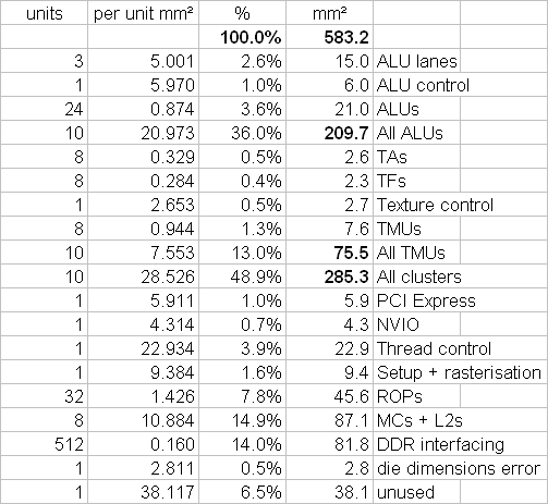
Here are my estimates for die usage for GT200 based on the high resolution GT200 die shot:

b3da022.png

I've measured areas inside major blocks on the die, ignoring the "shiny" spaces between these major blocks. This is because the shiny spaces vary in size and seem to indicate that there are only metal layers there, no logic. These shiny spaces amount to 38.1mm² of the die, that is 6.5% of the die appears to have no logic nor I/O :oops:

We can argue till the cows come home over the per-cluster split between ALUs and TMUs. Irrespective, the important thing to note is that a cluster is ~28.5mm².

On GT300, using 65->40nm scaling, a cluster of the same configuration (3 multiprocessors of 8 MADs, 2 MIs, 1 DP plus 8 TMUs) would be ~10.8mm².

Put bluntly, GT300 should have >3x the ALUs of GT200. ALU:TEX is very likely to increase, e.g. 4 multiprocessors per cluster, with 2 quad-TMUs. NVidia won't be able to reach 1024 ALUs, but I think somewhere in the region of 24 clusters (of 32 single-precision MAD ALUs ) = 768 is quite feasible. That would result in about 305mm² of clusters. Of course this is assuming no changes whatsoever. No increase in DP, no 32KB shared memory, and no other changes. Even after allocating 100mm² to ROPs and MCs (as opposed to 133mm² in GT200) there's still a hell of a lot of die left over, if GT300 is >500mm².


Some other entertaining numbers, just because I can, GT200 versus RV770, normalised to 55nm:
  • per single-precision MAD - 0.626mm² v 0.095mm² - 659%
  • per single texture result - 0.676mm² v 0.788mm² - 86%
  • per single colour write (ROP) - 1.021mm² v 0.808mm² - 126%
  • per single Z write (ROP) - 0.128mm² v 0.202mm² - 63%
Jawed
 
Last edited by a moderator:
On the cluster size?

I measured the components of a cluster for GT200 - the smallest measurement is 84 pixels. Whereas for RV770 it's possible to measure all 10 clusters in one go, where the smallest dimension is 893. The problem with the latter is that the components of an RV770 cluster include some inter-block shiny stuff (i.e. not logic). Whereas there's very little shiny stuff in the measurements of GT200. Though the short dimension for the GT200 ALUs measures 330 pixels and there are two thin shiny areas (splitting that block into its 3 separate multiprocessors).

So there's about 2-3 pixels error in 330 there and about 10 pixels error in ~900 pixels for RV770. So about 1% across the board in linear dimensions or a couple of percent in areas.

Jawed
 
OK but what we really know about GT300 for sure?

4X performance of GTX285? Any source? Maybe with Gflops but not in performance IMO.
We don`t know about real number of SP too.
Maybe i`m wrong but at the moment we don`t have many leaks about GT300 specs/supposed performance. :)

I'm pretty sure neliz was joking when he said 4x the performance. I'm expecting a best case scenario of 2x the 285's performance but I doubt it will go even that high on average. In some cases it might but realistically we can probably expect an average of about 80% faster in GPU limited scenario's. Hopefully it will be a bit faster overall than the 295. Which obviously puts it ahead of a 1600 sp RV7xx, i.e. the 4870 X2.

I'm a little behind the latest rumors on RV8xx, whats the highest end GPU supposed to be sporting there?
 
I'm pretty sure neliz was joking when he said 4x the performance.

Well yeah.. that was a yoke, I basically summed up all the rumours people seem to believe in now. i.e. GT300 is smaller than gt200@40nm yet double the performance. (i.e. about the size of G92 but packing double GT200 power)
I'm a little behind the latest rumors on RV8xx, whats the highest end GPU supposed to be sporting there?

pick a number from 16 to 2400 :D
 
TMUs can do BC6 (and obviously FP10/RGBE) at full speed, are structured custom, and run above 1GHz? (feel free to quote me on this in a few months even though it's certainly not a leak)
Ah yes, tis fun looking at old postings:

http://forum.beyond3d.com/showthread.php?p=1230016#post1230016

3T|120A|3R -> 0.6TFlops+ -> GT216/Late March
GT216 has 48 ALUs :p Still waiting to find out the rest of its specifications.

Maybe my >3x estimate for GT300 ALU capability over GT200 is looking rather foolish...

Jawed
 
Status
Not open for further replies.
Back
Top