You can't just increase clocks forever though simply because the power budget is there. If GF114 clocks @ 800MHz+ with a < 225W power budget, throwing 375W @ two of them doesn't necessarily yield 1GHz clocks.
No certainly not. I would only expect something like 750Mhz.
But the point is the opposite is true too at a certain point - you might not be able to really lower voltage (or only by a tiny amount) if you reduce clocks further, which means your perf/power might not improve at all if you lower clocks.
Sure there is, and it's been discussed on these forums. Many of the power components are shared, display controllers are not (usually) duplicated, and I'm sure there are other things as well.
Yes, but without any estimates how much power these shared things might save. My assumption is very little.
GF110 seems to be a good deal more power efficient than GF100, or at least it is more well-behaved at the limits.
Not really a whole lot - less leakage yes, most of the rest seems to come from better cooling.
Also, dual GF-114 may not be enough to beat Antilles, and I don't think that's a scenario Nvidia is comfortable with.
I'm just not sure GF110 is really more power efficient than GF114 (if they have their clocks/voltages set so they both draw about 150W). GF104 isn't quite as good on desktop nowadays, however that seems to be mostly because its voltages are set a bit too high (higher than on GTX 570 GF110 despite lower clock), of course that allows stellar overclocks but for power consumption it's a disaster.
Of course if you go for a 250W TDP target per chip, then it's a no brainer GF110 is better - you could increase voltages on GF104 but clock (and hence performance) wouldn't really go up a lot more, and perf/power sink way below GF110 level.
I never claimed any specific figures for the dual card though. All I said was that 375W seems like a lot for a mere dual GF114 SKU unless it's heavily overclocked.
I guess for a 375W card two GF110 gpus probably really would be more power efficient and hence faster. But it is possible the target TDP is 300W and it's just for overclocking headroom. And at 300W there might be very little performance difference between these two hypothetical solutions.
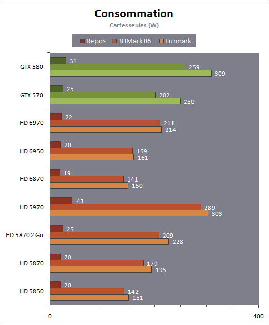
Look at HD 5870 vs. HD 5970. By this logic 5970 should be close to 2* 5870's TDP yet it is not. 5870 is 225W and 5970 is 300W.
The HD5970 is more of a 2* 5850 and it acts accordingly - twice the power draw, and very similar performance to HD 5850 CF. Not overvolting memory (as pretty much all other AMD desktop GPUs do) also helps a bit, as does using HD5850 chip voltages certainly.