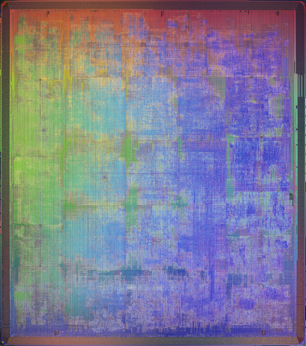
Look at this big 222 million transistor chip.....

Status
Not open for further replies.

Deadmeat

Banned
wafer.jpg

nV40 die shot.

Anand's estimation : Between 270~305 mm2.

In order to prevent it from burning up, nVIDIA was forced to DOWNCLOCK it to 400 Mhz for Ultra edition, from 485 Mhz of previous nV38. You just can't clock big chips with lots of transistors high...
 
uh, isn't that a wafer with NV40s on them?

here's a much better image, a close-up of the NV40 die
dieshot.jpg


to keep this console-related, it should be no problem for Sony to surpass this with Graphics Synthesizer 3 or Visualizer. not to mention ATI's two console VPUs for Nintendo and Microsoft.

I wonder how large and how stuffed with transistors the NV50 will be-and if it will come close to rivaling Sony's GPU for PS3.
 
Using .13, you forgot to note that, but I know what your trying to get at DM
Oddly enough, the transistor density of this IBM 130 nm process is HIGHER than SCEI's alleged "90 nm" process. So don't keep your hopes too high on SCEI fabs....

nV40 : 270~305 mm2 at 222 million transistors(0.82 million/mm2)
PSX2OAC : 90 mm2 at 55 million transistors(0.61 million/mm2)
 
NV40 = No Low-k, no SOI, .13...

what's the point of comparison between the NV40 and the BE?

Yes...i know the answer :?
 
Also considering that the EE+GS@90nm has 4MB of eDRAM which has higher density than logic, that 130nm process seems even better than I thought.
 
Why should it matter ? It is not like IBM is helping Sony and Toshiba with CMOS5 and CMOS6... oh wait, they have been and they still are.
 
...

Also considering that the EE+GS@90nm has 4MB of eDRAM which has higher density than logic, that 130nm process seems even better than I thought.
That's because

1. SCEI's design capability lacks behind indsutry leaders.
2. SCEI's fab capability lacks behind industry leaders.

And some Sony fans want us to believe that SCEI would pull off what Intel and IBM could not, a half a billion transistor clocking at 4 Ghz and burning so little power, yet produced inexpensively...
 
Re: ...

Deadmeat said:
Also considering that the EE+GS@90nm has 4MB of eDRAM which has higher density than logic, that 130nm process seems even better than I thought.
That's because

1. SCEI's design capability lacks behind indsutry leaders.
2. SCEI's fab capability lacks behind industry leaders.

And some Sony fans want us to believe that SCEI would pull off what Intel and IBM could not, a half a billion transistor clocking at 4 Ghz and burning so little power, yet produced inexpensively...

1. You seem to miss Toshiba and IBM in that analysis as they are both heavily helping SCE in terms of fabs and manufacturing technologies.

CMOS5 and CMOS6 are not been developed by SCE alone ;).
 
Status
Not open for further replies.
Back
Top