Larrabee: 16 Cores, 2GHz, 150W, and more...

B3D News

Beyond3D News
Regular
It is amazing how much information is out there in the wild, when you know where to look. TG Daily has just published an article partially based on a presentation they were tipped off about, and which was uploaded on the 26th of April. It reveals a substantial amount of new information, which we will not focus on analysing right now, so we do encourage you to read it for yourself.

Read the full news item
NOTE: Please discuss the architectural info on Larrabee in this thread, and the industry speculation TG Daily's article has in that other thread.
 
What of the possibility of a 3 operand x86 MADD?
It would fit mathematically with the 1 TF, clock speed target, and vector width.

edit:

Just reread slide 31.

Larrabee is listed as having 8-16 DP flops per cycle per core.
That seems counter to what has been rumored previously.

It also seems like Larrabee can handle non-SSE ops as well.
 
Last edited by a moderator:
Yeah, I was thinking a bit about that. I think what might actually make more sense for Intel is to be 3-wide: INT, ADD|MUL, ADD|MUL. So that way you can keep everything as being 2 operands, and you have a fair bit of flexibility anyway. If ADD was half-speed for DP and quarter-speed for MUL, it would also explain why it sports 8-16 DP Flops/cycle, rather than just 8 or 16. That would also imply SP would be 32/cycle, but that's just speculation.

One thing I'd like to highlight is that slide 17 uses a standard CSI x86 infrastructure with no traditional CPU on any of the sockets. Considering each chip only has one kind of core apparently, this implies that each core is apparently able to run a modern operating system.
 
It seems Larrabee will be running full x86 threads. It seems curious, though, that the L1 latency is only 1 cycle.

Gesher has a 3 cycle latency, so I wonder how they can reduce it so much for Larrabee.

If Larrabee's vector unit has ADD and MUL pipes, it would explain why a unit that is characterized as being 512 bit can support a throughput that would require 1024 bits per cycle per operand.
 
:oops: How long before some smartass tries to run 16 different OS's on this kit...?
Well, the CSI version has 24 cores according to the same slide, actually, and 96 threads. Assuming that proper virtualizaton is supported (which I kind of doubt, but heh), that would be quite a sight to behold indeed, hehe.
 
from the presentation

I fail to understand how a multiplier (no matter how many bits) can take 150,000 gates to implement.
 
Wasn't that the 80-cores one? From 80 to 16...

The "Terascale" project had little to do with "Larrabee", other than both being multi-core CPU designs. The "Terascale" did use 80 cores on a single die alright..., but each of them had a very simple, non-x86 design.
This is the magic of Larrabee, a possible "x86 chip optimized for 3D graphics and GPGPU apps in need for floating point power" of some sort.
Kind of like a Cell BE, but with a more homogeneous design (i.e., all cores have a similar design, whereas Cell has a main general purpose PPC core and eight -PS3 has seven, of course- specialized cores).
 
Last edited by a moderator:
Very interessting view in Intels GP"GPU" and CPU future:
geshervslarabeear9.jpg


:D
 
It seems Larrabee will be running full x86 threads. It seems curious, though, that the L1 latency is only 1 cycle.

Gesher has a 3 cycle latency, so I wonder how they can reduce it so much for Larrabee.

Well for one thing Larrabee has twice the cycle time, so in absolute terms it's not that huge a reduction (dunno if that's particularly relevant...). Still, didn't p4 have a 2 cycle load-use latency on its L1 (possibly enabled by the small L1 size)? Does anyone know the how Core 2 does in this area?
 
Very interessting view in Intels GP"GPU" and CPU future:
geshervslarabeear9.jpg


:D

So Geshers not out for another 3 years and Intel are already releasing slides showing how slow it will be? Lol :LOL:

Actually at the moment Gesher interests me a lot more than Larrabee. Sure its only got 1/5th the floating point performance but 224 GFLOPs DP is nothing to sneeze at and I assume it would be double that in SP. Plus Gesher should have outlandish single threaded performance which is something that seriously worries me with Larrabee.
 
At this point i'm a little confused...

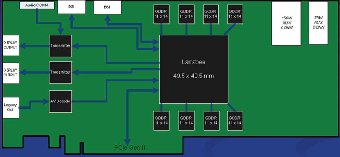
intel-larrabee-01-pdf.jpg


Photo taken from http://xtreview.com/addcomment-id-2572-view-Intel-larrabee-and-processors-sandy-bridge-(Gesher).html
And http://xtreview.com/images/davis.pdf

So Gesher is basically an advanced ClearSpeed copro card/Torrenza and Larrabee will be a sock-able CPU? Then that picture is wrong? It seems larrabee is the GPU then?? ( see the AV decoder, display input etc... seems a graphics card... )

Is the Larrabee some general x86 multi cores(for example 4) + some SIMD-math-dedicated cores(12-20) or just a CPU with 16-24 general purpose x86 cores? Am gonna be able to program it using OpenMP then?

The presentation is too confusing ( mix 80-cores + Gesher + Larrabee >< + GPU + !!$##@ ). I think the 80-cores is, indeed, the GPU. The Gesher is oriented like Torrenza copros plugged using PciE and Larrabee is a 16-24 general purpose x86 sockable-cpu but who know...!

And perhaps the Larrabee and Geshes will be general purpose, so can be used a CPU, GPU, sockable coprom PCIe card or whatever. Multiple configurations of the same thing.

Btw, I saw Intel could use GDDR5 for this.

And to finish a thought... are we going to return to software rendering then?
 
Last edited by a moderator:
I think that last slide with the green PCB schematics must be a fake and/or misinterpreted from official info.
The Intel slide above that clearly mentions "CSI" as the bus/connector of choice for either "Larrabee" and "Gesher", but this one says "PCI Express Gen II" (2.0).
Last time i checked they were not one and the same thing, unless CSI has something to do with "Geneseo".
 
Back
Top