Is it possible the new X360 model has shrunk chips? (X360E)

I'll eat my words on the size (grumble grumble). :p

There are a couple capacitors that have been removed now (one to the left of the package, and one north of it). There's another one that was removed in the north-west corner, but that's probably related to the change in rear connectors. Also... no ring of light, no speaker (bottom left) and maybe a couple other related items in the bottom right... They ditched HANA (no multi-AV/spdif port so...).

360S
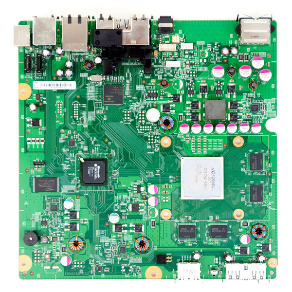
nakedboard.jpg


360E

shHjU8S.jpg


Southbridge moved up a bit... some stuff on the left removed. Package size looks fairly similar (lines up with the capacitors). Funny they moved the crystal oscillator. Some other misc items removed (unmarked).

They shifted the power connectors for one of the drives and the fan for some reason too.

-----

Curiously, the power connector is different.
 
The PS3 shrunk without any changes to the chips. Plus the new 360 doesn't look very small.

i think it looks fairly small in the ifixit guy's hands.

it's a gradual thing, slim wasn't just way smaller than elite, but the difference was significant. probably again the case with this versus slim, and now overall it's pretty small (slim already isn't exactly huge)

EeraEQMfXKQXjT31.medium


i wonder where ifixit got there's, have not seen one on amazon which is where i thought they'd be first out of pure logistical ease. guess they just found one in a store.

oh well i see an anand editor and df discussing this teardown on twitter, so maybe anand will do a better breakdown eventually.
 
i wonder where ifixit got there's, have not seen one on amazon which is where i thought they'd be first out of pure logistical ease. guess they just found one in a store.

Best Buy Canada has them online so I expect other retail outlets do as well.

<edit> now it says preorder stock on monday, guess they did not have many.
 
Curiously, the power connector is different.

Pity they (iFixIt) didn't look at the power brick and see if it is lower power now. That would perhaps be the most solid answer on shrink (power consumption).

Sounds possible if the connector changed.

Else wait for someone to take the heat spreader off.
 
IBM was absolutely involved on this.

I guess I need to rephrase: The chip wasn't manufactured by IBM, though from what you and willard are saying they helped create this version of it. That is what I was trying to say. Sorry for the confusion, I was not feeling too well when I posted that.
 
Xbox 360E - Slim redesign

Xbox 360 E unboxing & comparison to Xbox 360 S...


It's barely smaller than the 360 S. I think this one will be more appealing when they do the price drop. I think I will hold off a tad longer.

Tommy McClain
 
Most likely. :) Too bad there was no hotchips presentation. I'm just a little curious about how they deal with the HSIO bus, but more importantly just a die shot to see how things progressed again (since they included 90/65/45nm shots last time).
 
I guess MS are too focused on the present to want anyone looking back to the 360 ... :(

Makes you think though. If a 32nm SoC, complete with edram and a super clocked (relative to 4Bone) CPU was available after all, then that that great big hunk-o-chunk-o-esram in the Bone seems kinda expensive. That 32 MB would be tiny on this process. A daughter die with stupid amounts of 32 nm edram might have worked too - avoid that cumbersome DDR3 bus.

Also, Nintendo Y two separate 45nm chips, both with edram, when MS found this cheaper? BOMed back to the stone age.
 
Makes you think though. If a 32nm SoC, complete with edram and a super clocked (relative to 4Bone) CPU was available after all, then that that great big hunk-o-chunk-o-esram in the Bone seems kinda expensive.
It helps to have a relatively small chip with circuits that are either slow in the case of the GPU or are speed demons with very simple and poorly performing pipelines like Xenon. Those architectures are pretty well understood by this point.

It might be that the incremental cost of the more expensive 32nm SOI process for a small chip was better than a more complex package with the daughter die.

A daughter die with stupid amounts of 32 nm edram might have worked too - avoid that cumbersome DDR3 bus.
eDRAM is denser, perhaps 2-4 times as much, but that's very far short of 8GB of DDR3.
 
48Mb would suffice I think. Also as Cerny said with eDRAM they could get 1Tb bandwidth.

PS3 also got smaller RSX on latest MB.
 
It might be that the incremental cost of the more expensive 32nm SOI process for a small chip was better than a more complex package with the daughter die.

That's a good point. Would seem to go for the WiiU too, though...?


eDRAM is denser, perhaps 2-4 times as much, but that's very far short of 8GB of DDR3.

I was thinking more along the lines of 128 MB or so. Enough for all buffers and for a texture cache covering all re-usable texels for one frame to the next. That should buy you the ability to shift from a 256-bit to a 128-bit DDR3 bus (given that it's DDR3 2133) and reduce board area dedicated to equal length traces, and that would also allow you to halve the number of memory chips on the board (1GB DDR3 is now entering mass production).
 
Makes you think though. If a 32nm SoC, complete with edram and a super clocked (relative to 4Bone) CPU was available after all, then that that great big hunk-o-chunk-o-esram in the Bone seems kinda expensive.

As 3dilletante mentioned above, it's a different situation considering die size & 2 chips vs 1 cup. SOI is a bit more expensive than bulk, but eDRAM also has its costs on top of that since it's done in two steps for fabbing it alongside regular logic. That means it takes longer to produce the final chip, and if you think about the yield issue, they have to first produce usable eDRAM, and then they have to produce functioning logic in the next step.

There's this density comparison between 28nm and 32nm SOI, and I imagine for Durango, it might have ended up being a wash if not worse to use 32nm SOI for overall die size (porting jaguar & GCN from bulk to SOI libraries).

Also, Nintendo Y two separate 45nm chips, both with edram, when MS found this cheaper? BOMed back to the stone age.

I suspect heavily that the "edram" in Latte is simply MoSys 1T-SRAM, not actual DRAM with capacitors and such. I would not put it past Nintendo to keep re-using some license agreement from 15 years ago. ;)

Espresso... that should be real eDRAM through and through. Their using 45nm probably had to do with pad limitations to an extent, I mean, the die shot has a considerable amount of dead space. I'm sure it was still cheaper than 32nm SOI eDRAM in 2012 though. The fact that they even extended the Gamecube CPU to three cores is hilarious enough with the mismatched L2, not even an L3 shared cache.
 
Last edited:
Back
Top