Intel "Ice Lake" (10 nm)

What do they mean, "re-introduce"?

Since when did the integrated regulator go anywhere?
 
I think that's complete bollocks. Intel's latest power saving modes rely entirely on the FIVR, and wouldn't work without it. I doubt they could hit even lower power consumption figures than Broadwell without it.
 
Well, Skylake not having a FIVR does seem unbelievable to me, too. However, I do not work for Intel :)
 
No, not there. It originated somewhere else, though with the same slides showing multiple voltages being supplied to Skylake.
And the justification was also different from WCFTech's silly "did not pay off", it was that Skylake was designed by the other team or had been in design for too long a time, and Intel simply had not had the opportunity to integrate a FIVR in Skylake. It would be making a return later, however.
 
It seems it will take a while for Intel's 10nm process to match—and especially overcome—the speed of their current 14nm++:
intel_process_perf_scaling.png


Power scaling looks great, though. I guess that means plenty of great Ice Lake laptops, but desktop chips may stick to 14nm++ for some time (or 14nm+++?) unless Ice Lake's micro-architectural improvements are sufficient to make up for its slower transistors.
https://newsroom.intel.com/newsroom...ites/11/2017/03/Mark-Bohr-2017-Moores-Law.pdf

(This is a few months old, so my apologies if it was already posted somewhere. Also, those dotted lines are, err, let's go with "an optimistic interpretation of the data".)
 
Power scaling looks great, though. I guess that means plenty of great Ice Lake laptops, but desktop chips may stick to 14nm++ for some time (or 14nm+++?) unless Ice Lake's micro-architectural improvements are sufficient to make up for its slower transistors.

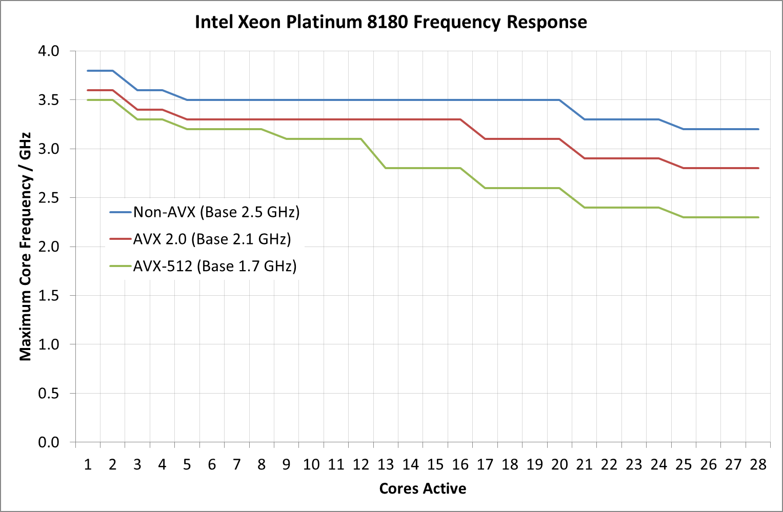
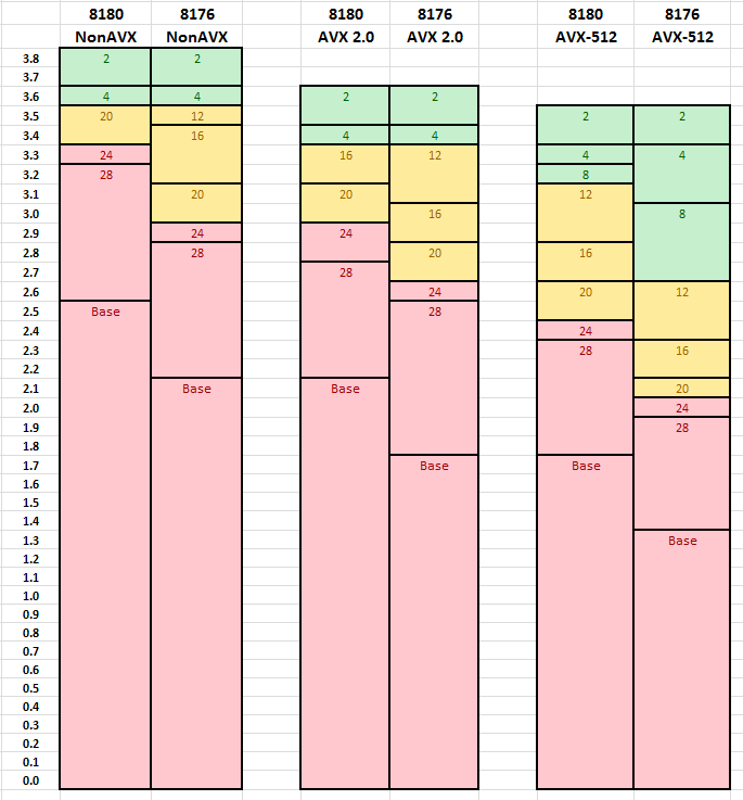
Every AVX-512 processor would be better off on 10nm because it would remove the need for reduced base and turbo frequencies.

Even workloads that don't do floating point with AVX-512 would benefitsince some c stdlib function will use AVX-512 move instructions for memory copy/moves; AVX-512 move instructions impose AVX-256 clocking restrictions on the core. So while your memory moves and copys are almost twice as fast, the rest of your code suffer a 10-20% penalty.

I think the whole AVX downclocking mess is a result of process projections not quite panning out. The process people over-delivered on speed, but under-delivered on power consumption.

Cheers
 
Are those clocking restrictions rigidly applied when AVX-256/512 instructions are decoded, or just normal throttling?
 
From Heise.de: "Xeon Phi is dead, long live the Xeon-H" (original).

(Google Translate) said:
2019/20 will then follow the Ice Lake Scalable Xeons (ISX-SP) in 10 nm +, with up to 38 cores, eight memory channels and up to 32 GB of High Bandwidth Memory (HBM2) on board. But one hears from a moderate bandwidth of 650 GB / s - for comparison: NEC Aurora creates with HBM2 1.2 TB / s.
I was expecting ~50 cores but it looks like I was far too optimistic.

The memory bandwidth is a bit odd, since it and the memory capacity implies 1.27 Gbps HBM2 for four stacks or 2.54 Gbps HBM2 for two stacks (or some strange configuration). Current high end GPUs use 16 GB HBM2 at 480-900 GB/s. If high end CPUs with HBM tend to require similar or more HBM capacity than high end GPUs, then I think four stacks are more likely than two. If so, then the low memory clocks could be explained by CPUs generally requiring less bandwidth than GPUs. I doubt cost is an issue for the largest Xeons anyway. Thoughts?

There's also a mention of a 24 core "normal" Icelake which seems to be the mid tier chip.

Also, a version of Icelake is planned as a Xeon Phi replacement:
(Google Translate) said:
The normal Xeon SP line is then to be extended by a special version ISX-H (codenamed Knights Cove) with 38 or 44 cores, which is intended as a successor to the Xeon Phi. […] The 44-Kerner should be an MCM consisting of two chips of 22 cores.
I'm surprised that ISX-H doesn't have many more cores than ISX-SP.
 
Last edited:
From Heise.de: "Xeon Phi is dead, long live the Xeon-H" (original).

I was expecting ~50 cores but it looks like I was far too optimistic.

The memory bandwidth is a bit odd, since it and the memory capacity implies 1.27 Gbps HBM2 for four stacks or 2.54 Gbps HBM2 for two stacks (or some strange configuration). Current high end GPUs use 16 GB HBM2 at 480-900 GB/s. If high end CPUs with HBM tend to require similar or more HBM capacity than high end GPUs, then I think four stacks are more likely than two. If so, then the low memory clocks could be explained by CPUs generally requiring less bandwidth than GPUs. I doubt cost is an issue for the largest Xeons anyway. Thoughts?

There's also a mention of a 24 core "normal" Icelake which seems to be the mid tier chip.

Also, a version of Icelake is planned as a Xeon Phi replacement:
I'm surprised that ISX-H doesn't have many more cores than ISX-SP.
38 cores?
Merely 38 cores?
Sounds pretty meh.
Especially if the rumors of Rome are true.
 
Slide3.png

from that slide intel claimed 10nm have 100.8 Mtr/mm2 or 2.688x density improvement against 14nm. but after i count 14nm broadwell density from broadwell dual core only 15.85 Mtr/mm2(82mm2 and 1.3billion transistors). amd raven ridge 14nm 2700u have better density 23.59 Mtr/mm2(209.78 mm2 and 4.95 billion transistors). why intel claimed very far from reality?

if i multiply 15.85 with 2.688x density improvement, intel 10nm only have 42.6Mtr/mm2 denisty, that's value below tsmc 10nm chip a11 that have 49.05Mtr/mm2(87.66mm2 and 4.3 billion transistors)
 
Last edited by a moderator:
Because Intel is likely quoting transistor density of some highly regular, high density structure, like SRAM. A CPU is a very different beast.

Intel doesn't have as high density as the foundries at similar nodes because the foundries support manhattan routing in the entire stack, whereas Intel's lower layers are alternating north-south or east-west in order to increase manufacturability.

Cheers
 
Guy mentioned a dual core die as basis for calculations, which means core/IO ratio is pretty much as low as it goes with intel chips these days.
 
Guy mentioned a dual core die as basis for calculations, which means core/IO ratio is pretty much as low as it goes with intel chips these days.
Intel Xeon E5-2600 v4 Series with 22cores/44threads have density not far from dual core 15.78 Mtransistors/mm2(7.2billion transistors and 456.12mm2).

i just realized why intel graphics is so bad in area size if compared amd and nvidia@14nm. from broadwell(14nm) gt2 to gt3 intel add 51mm2 with only 600million transistors grow equal to 11.76Mtransistor/mm2 for graphics density.
 
Last edited:
Back
Top