ELSA hints GT206 and GT212

Arguably GT21x GPUs were designed before the shock and awe of RV770 hit, so what are the chances NVidia will respond specifically by increasing ALU:TEX?
"Specifically" almost nil, though I am not sure how modular their TPCs are and if they had plans in the drawer for various ALU:TEX-ratios.

But chances are, if they didn't think of increasing that rate by themselves and before Q2/2008, we're not going to see any drastic change.

OTOH seeing the massive overhead they're having with their (scheduling-) logic outside of TPCs, it would be almost foolish for them not to be carrying that burden without thinking of it as an investment in future GPUs.
 
Are you referring to the "Pixel Setup" data point in figures 13 and 14 in the Siggraph paper? That's about 10%.
I'd need to find it again, but I think it varied from 10 to 25% depending on the game. Of course my memory could be very faulty indeed :) Either way, it's not negligible, so it's not a straightforward "We should remove this" even if it did make sense in practice.

And, I'm still looking, high and low, for any sign of a transcendental ALU in Larrabee.
Presumably they've got an instruction or two to make it a bit cheaper, but not a dedicated instruction per-se?

Well, forgetting the register file for a second, all ALU operands have to come through the operand collectors, whether they're from the register file, shared memory, the constant cache, video memory or attribute parameter buffer.
But that's a much lower die size penalty than having to try hiding register bandwidth limitations for real-world scenarios. Also some of that complexity must surely be there anyway for shared memory, as required by CUDA.

Regardless, the operand collector is still bigger simply to deal with the increased bandwidth of a MAD+MI configuration.
You mean the register file bandwidth? (since the others clearly aren't really affected by it).

The way I see it both are legacies of GPU history, accelerated interpolation was a key part of getting texturing to work when most rendering cycles were texturing bottlenecked and fast transcendentals were needed to get vertex shading at decent speeds (especially given how few vertex pipes there were).
I'm not sure I agree completely; how many interpolation operations nowadays are directly for the registers that'll be used for texture fetches? It has already moved past that goal and is still useful.

As you say, the real question is how useful it is - or more precisely, how much does its usefulness *vary*? Because if it's always not-very-useful, you can just make it less powerful but cheaper. If sometimes it's very useful and sometimes completely useless and wasted, then it starts making some sense to unify that functionality into another block. However being able to extract a little bit of the MUL clearly already helps that problem a bit (but only if adding the MUL on its own makes sense; otherwise it's less of a win).
 
I'd need to find it again, but I think it varied from 10 to 25% depending on the game. Of course my memory could be very faulty indeed :) Either way, it's not negligible, so it's not a straightforward "We should remove this" even if it did make sense in practice.
In the paper the performance data is collected by simulating Larrabee cores - so the ~10% cost of Pixel Setup on those graphs is using whatever ALUs they are planning for Larrabee.

Maybe there is a transcendental ALU and maybe there's an attribute interpolator too, but there's no mention of either of these things so far as I can tell.

Presumably they've got an instruction or two to make it a bit cheaper, but not a dedicated instruction per-se?
I can imagine a look-up table instruction to seed the transcendental macros with the data they need to start:

http://developer.intel.com/technology/itj/q41999/pdf/transendental.pdf

where double-precision vec2 MAD ALUs can calculate DP transcendental functions. A vec2-DP ALU can do any transcendental in 52-72 cycles, which is a throughput of 1/104 to 1/144. So in Larrabee a SIMD-16 would have a throughput of 1/26 to 1/36, again for double-precision. I dunno how much faster single-precision would be. Twice as fast? : 1/13 to 1/18.

GT200 currently has 1/4 to 1/8 throughput (maybe there are some things that are 1/16). Halving those again (as you propose) produces 1/8 to 1/16 - very much like the rate for Intel's macros on IA-64, translated onto Larrabee.

Though of course NVidia's pair of SIMDs (MAD-8 and MI-4 - MI-8 is capable of 2 transcendentals or 8 interpolations per clock, so MI-4 is half) is more like half the width of Intel's SIMD-16.

But for overall throughput, wouldn't you rather have one SIMD-16 than two MAD-8s and two MI-4s? Sure, transcendentals are faster in the latter, but the SIMD-16 is smaller, once you take into account the control overhead of the operand collectors and the 4 SIMDs in NVidia's architecture, not the one in Larrabee.

But that's a much lower die size penalty than having to try hiding register bandwidth limitations for real-world scenarios. Also some of that complexity must surely be there anyway for shared memory, as required by CUDA.
Yes to both those points. But there's still dedicated scoreboarding for MI operands - they still have to be scheduled and tracked.

You mean the register file bandwidth? (since the others clearly aren't really affected by it).
Operand and resultant bandwidth has to be managed regardless of the ALU lanes involved.

I'm not sure I agree completely; how many interpolation operations nowadays are directly for the registers that'll be used for texture fetches? It has already moved past that goal and is still useful.
Yes, but D3D10 only allows 16 attributes per vertex, while D3D10.1 allows for 32 attributes. So, per fragment, the worst case interpolation is currently 32 32-bit values.

A single G92 cluster can interpolate 16 attributes in 1 cycle (2 multiprocessors, each doing 8 per clock). The desired rate is set by the rasteriser/fillrate, not by ALU throughput. In other words, G92's rasterisation rate of 16 fragments per core clock is supported by an interpolation rate of 128 attributes per ALU clock, so in 9800GTX at 675/1688, that's a 1:20 ratio, rasterisation:interpolation.

GT200 rasterises at 32 per core clock and interpolates at 240 per ALU clock, so GTX280 602/1296 has a 1:16 ratio.

A speculative, small, GT300 with 384 interpolations-per-clock (384 MAD lanes) with say 4:1 ALU:TEX, and with say 600/1300 clocks would be 1:26. Why? :oops:

ATI gets by with 32 interpolators, or 1:2.

So, yes, my conservative GT300 has way way too much interpolation rate, so halving the MIs or dropping them entirely really sounds like a good idea.

If deleting MI allows GT300 to go from 4 to 5 multiprocessors per cluster, that would be a bonus eh?

As you say, the real question is how useful it is - or more precisely, how much does its usefulness *vary*? Because if it's always not-very-useful, you can just make it less powerful but cheaper. If sometimes it's very useful and sometimes completely useless and wasted, then it starts making some sense to unify that functionality into another block. However being able to extract a little bit of the MUL clearly already helps that problem a bit (but only if adding the MUL on its own makes sense; otherwise it's less of a win).
Clearly the MUL was a complete waste of time until GT200 arrived - and the compilation and instruction-dependency scoreboarding issues it generates are hardly a decent pay-back for the shitty utility.

The reality is that interpolation is bloody cheap the way NVidia's done it, by tacking it on the side of transcendental. Going forwards, though, it looks like a case of the tail wagging the dog

ATTF1010.jpg

So the intriguing question is, does interpolation explode in your face if the MI is dropped? Seeing the stratospheric interpolation rates of even G92, I don't see how NVidia can justify keeping it in future.

(I'm actually wondering if I've radically misunderstood interpolation rates in NVidia's architecture because the numbers are so silly.)

Jawed
 
Which of those is an ALU-specific test? I know 3DMark06 Perlin Noise is ALU-bound (just about).

On the Nvidia hardware I've had the two Perlin Noise tests are pretty much 100% shader bound and the POM tests significantly so despite the texturing happening there. And what else do you propose is happening with the GS tests that would limit performance besides ALU throughput?

HD4870 can't get any slower than the serial MAD test I linked, i.e. 68% performance per mm2 or 37% of the absolute performance of GTX285.

As to the "nature" of more general code, the issue is really about the memory system. Some general code is so compute bound it barely uses any kind of memory resources, either video RAM or on-die shared RAM - just registers, basically. That code will be quite happy in naive scalar form.


Oh your percentages were normalized per mm. Misread them. The memory issue is a fair point and it was raised in that paper you linked above. But isn't that an implementation detail? I'm sure there are cache structures that work well for scalar issue.

Eh? Until AMD re-writes the core to use LDS/GDS, F@H tells us precisely nothing.

Oh my bad, I thought they were doing so already....and why does AMD have to rewrite the core? What's stopping the stanford guys from doing so?
 
so gt300 just a die shrink to 40nm from gt200?

why not? who cares about graphiccards anyway? i myself got a xbox and just LOVE the fact that i'll be TOP NOTCH performance and hardware wise until the earliest of 2012!

a proud GAMER!
 
On the Nvidia hardware I've had the two Perlin Noise tests are pretty much 100% shader bound and the POM tests significantly so despite the texturing happening there. And what else do you propose is happening with the GS tests that would limit performance besides ALU throughput?
Shader bound on NVidia doesn't mean shader bound on ATI.

3DMark06 Perlin Noise, while ALU bound on ATI, won't be ALU bound if ATI increases the ALU:TEX of the hardware even a smidgen, say to 5:1.

The GS tests seem to do a lot of "texturing", i.e. reading data from memory, as far as I can tell.

Oh your percentages were normalized per mm. Misread them. The memory issue is a fair point and it was raised in that paper you linked above. But isn't that an implementation detail? I'm sure there are cache structures that work well for scalar issue.
Yep, you'll find them in CPUs.

Oh my bad, I thought they were doing so already....and why does AMD have to rewrite the core? What's stopping the stanford guys from doing so?
Mike Houston appears to be the one "writing the core". Originally he was a Stanford guy writing Brook, but now he's an AMD guy writing Brook+. The core is, as far as I can tell, a platform for the Stanford guys to codify the molecule simulation they want to run - sort of a library I think.

Maybe Stanford has guys writing Brook+, too, dunno - I don't understand the organisation of their programming teams. But I think Mike's responsibilities extend into the functionality of Brook+ itself, i.e. how it's compiled to run upon IL. I'm not saying he's a one man band or anything, merely that between a F@H core and AMD hardware there's several layers, and LDS/GDS functionality is lost in there somewhere...

The first step is to get IL using LDS/GDS (maybe that works already?) and then extending Brook+ so that it correctly targets LDS/GDS within IL.

Why not drop Brook+ and just write the core in IL? Dunno... What about OpenCL?...

Jawed
 
The reality is that interpolation is bloody cheap the way NVidia's done it, by tacking it on the side of transcendental.
Cheap in terms of arithmetic logic, not data flow. Compared to ATI's top of the pipe attribute interpolation, storage and data flow costs are huge.
(I'm actually wondering if I've radically misunderstood interpolation rates in NVidia's architecture because the numbers are so silly.)
I think you have, because they're not high enough to support the TMUs in G92 for straight bilinear, IIRC.
 
Cheap in terms of arithmetic logic, not data flow. Compared to ATI's top of the pipe attribute interpolation, storage and data flow costs are huge.
I was tempted to waffle on this subject earlier, but didn't.

Assuming that ATI stores all the fully interpolated attributes per fragment (figure 7):

http://ati.amd.com/products/radeonx800/RadeonX800ArchitectureWhitePaper.pdf

Once the visible pixels have been determined, the next step is to assign them initial values for basic parameters such as color, depth, transparency (alpha), and texture co-ordinates. The initial values are determined by looking at the values assigned to each vertex of the current triangle, and interpolating them to the location of the current pixel. The interpolated values are stored in registers that are used by the pixel shader units.

then I guess the worst case scenario (32 attributes per fragment) must cause a drastic reduction in fragments in flight, along the normal lines of register file trade-off for registers-per-fragment versus fragments-in-flight.

It seems it doesn't take many attributes per vertex to really hit the register file allocation per fragment, e.g. I can imagine 8x fp32 (2x vec4) is reasonably common. Naturally some of these can be freed-up if they contain texture coordinates, once the texture coordinates have been consumed.

I suppose register file storage of pre-computed interpolated attributes would also explain the strong bias in ATI towards a large register file.

In NVidia it seems to me that the extra data path to fetch interpolant data is a real issue, as you mention. i.e. there's an interpolant buffer which the operand collector must fetch from, and then schedule, for issue to MI.

That's a fair bit of bandwidth. I think the fetch bandwidth is 5x 32-bit (A, B, C, x, y are all 32-bit) per quad, and it generates 4x fp32 interpolated attributes. Multiply by 2 for the entire SIMD-8 MI. Or call it 1.25 scalars fetch bandwidth per attritube per clock and 1 scalar per attribute per clock resultant bandwidth.

The data paths in NVidia (register file, constants, shared memory, interpolants, RAM) sure look messy when compared with the clean L1/register file model in Larrabee.

Yet another target for a radical clean-up in GT300?

I think you have, because they're not high enough to support the TMUs in G92 for straight bilinear, IIRC.
:oops: Higher is even sillier. You sure? (I once thought the same, too.)

The ALUs are >2x TMU clock rate, and each multiprocessor can generate a 2D texture coordinate for 4 fragments in one ALU clock (8 attributes per clock), so G92 has > twice the interpolation rate required for bilinear. What am I missing?

Jawed
 
Jawed said:
So, per fragment, the worst case interpolation is currently 32 32-bit values.
That should be 32 vector interpolants, or 128 scalar 32-bit values.
 
The data paths in NVidia (register file, constants, shared memory, interpolants, RAM) sure look messy when compared with the clean L1/register file model in Larrabee.
Hmm, that list may well be shorter: interpolants could be held in shared memory.

Jawed
 
The data paths in NVidia (register file, constants, shared memory, interpolants, RAM) sure look messy when compared with the clean L1/register file model in Larrabee.

Would the current texture cache be a good candidate for conversion into a generalized per-cluster L1? It can then serve as a texture/constant/global memory cache. And is there documentation that points to dedicated interpolant storage on Nvidia's hardware - why wouldn't they just reside in the register file?

Larrabee's L1 looks clean if you're listing it out like that but the implementation and accesses to that L1 are certainly much messier and more complicated than Nvidia's multi-banked shared memory approach.
 
Would the current texture cache be a good candidate for conversion into a generalized per-cluster L1? It can then serve as a texture/constant/global memory cache.
Don't think so, the L1 is currently very precisely targetted at serving texels, in fairly complicated access patterns, to the texe fetch/filtering stages.

The shared memory (PDC) might be.

For what it's worth Larrabee's dedicated texture units have their own cache.

And is there documentation that points to dedicated interpolant storage on Nvidia's hardware - why wouldn't they just reside in the register file?

OPERAND COLLECTOR ARCHITECTURE

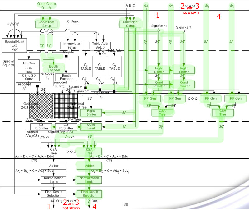
[0066] FIG. 7 is a block diagram of another exemplary embodiment of the Register File Unit and Execution Unit(s) of FIG. 2, in accordance with one or more aspects of the present invention. Register File Unit 750 and Execution Unit(s) 770 perform the functions of Register File 250 and Execution Unit(s) 270, respectively. A Collector Unit 730 receives operand addresses and corresponding program instructions for execution by an Execution Unit A 765 from Register Address Unit 240. In some embodiments of the present invention, Execution Unit A 765 is configured to perform interpolation, reciprocal, square root, multiplication, logarithm, sine, cosine, and power function operations. In particular, Execution Unit A 765 may be configured to execute program instructions with up to two operands. For some of the program instructions two operands are read from one or more banks 320. For other program instructions two operands are read from another storage unit (not shown) that stores per primitive values, such as triangle attributes, plane equation coefficients, and the like. Additionally, two operands can be read from a combination of the per primitive value storage unit and Banks 320. Access to the per primitive value storage unit is arbitrated since more than one Collector Unit 735 and/or 730 may request access in single cycle.

Larrabee's L1 looks clean if you're listing it out like that but the implementation and accesses to that L1 are certainly much messier and more complicated than Nvidia's multi-banked shared memory approach.
Why?

Do you mean the software threading model and cache misses? I certainly have some qualms there, but current GPUs have large functional blocks that are idling very often and I think that that wastage is far worse than the instantaneous hardware-thread switching overhead that Larrabee will suffer.

Jawed
 
In NVidia it seems to me that the extra data path to fetch interpolant data is a real issue, as you mention. i.e. there's an interpolant buffer which the operand collector must fetch from, and then schedule, for issue to MI.
Some comments in this forum actually suggest that G80 onwards has multiple post-transform vertex caches, and if more than one multiprocessor is working on the quads from a polygon, its vertex attributes are copied to each.

It's hard to say which method is best. NVidia would use less space for attributes, but would need a separate storage area for attribute data and another data path into the shader units. ATI gets dual use out of its register space, and I think register-heavy shaders tend not to use the iterators much (in the case of GPGPU, almost none), and super-high interpolator use is pretty rare. From that perspective, the storage cost is almost free if you're already designing a GPU capable of handing a high register load.

ATI's method seems cleaner to me. No need to worry about interpolation in the shader core, as it's already done.

:oops: Higher is even sillier. You sure? (I once thought the same, too.)

The ALUs are >2x TMU clock rate, and each multiprocessor can generate a 2D texture coordinate for 4 fragments in one ALU clock (8 attributes per clock), so G92 has > twice the interpolation rate required for bilinear. What am I missing?
I thought each multiprocessor can generate a 2D texture coordinate for only 1 fragment per ALU clock, because it's quarter speed. I see that the B3D review says that they're full speed, but that doesn't make sense according to the multifunction interpolator design. If it's quarter speed at doing f(X) = C0 + C1*X + C2*X^2, then it'll be quarter speed at doing U(x,y) = A*x + B*y + C.

:oops: - well that puts quite a dent in ATI's register file, allowing only 8 batches in flight and assuming at least one register can be clawed-back on the first instruction executed :p
Well, that's a worst case scenario. Nobody uses anywhere close to 128 attributes. The other thing to note is that often attributes are only used once in a program, particularly when you have so many, so the register they occupy is freed as the program progresses; likewise, you don't need all registers to be available at the beginning of a program.
 
Last edited by a moderator:
why wouldn't they just reside in the register file?
Vertex attribute access doesn't match the behaviour of register access, nor are the units writing the data the same.

When you have batches of 32 processed by 8-SIMD units, no register location needs to be read/written more than once every 4th clock, because each register is only used for one pixel, and there are savings to be had in designing the register file with this constraint in mind. Attributed data, on the other hand is used for possibly all pixels in a batch. The other difference is that the attribute data is written to each cache from the setup engine, whereas register data has no need to have an external connection except to pass the final pixel info to the ROPs.
 
Some comments in this forum actually suggest that G80 onwards has multiple post-transform vertex caches, and if more than one multiprocessor is working on the quads from a polygon, its vertex attributes are copied to each.
The latter seems inevitable. No one seems to have worked out what's happening with the routing/scheduling of geometry.

It's hard to say which method is best. NVidia would use less space for attributes, but would need a separate storage area for attribute data and another data path into the shader units. ATI gets dual use out of its register space, and I think register-heavy shaders tend not to use the iterators much (in the case of GPGPU, almost none), and super-high interpolator use is pretty rare. From that perspective, the storage cost is almost free if you're already designing a GPU capable of handing a high register load.
I suppose it's a question of the cost of the interpolators. Each interpolator is a MUL and an ADD running in parallel:

Vertex data processing with multiple threads of execution

My first thought is that's a 64-way MIMD configuration for RV770's 32 interpolators (32x2). But I think it should be possible to SIMD-ise that, e.g. 4x32.

ATI's method seems cleaner to me. No need to worry about interpolation in the shader core, as it's already done.
I'm thinking that G80's MI design, where transcendentals and interpolations share an ALU and at least some data paths is a good solution for an intermediate period before they junk MI. It seems to me that utility can only decrease with time, as the per-fragment cost of interpolation falls off with more and more complex pixel shaders (and the increasing cost of non-pixel shaders) and the proportion of transcendental calculations in general computational code seems to be not high enough to warrant building dedicated transcendental ALUs.

I thought each multiprocessor can generate a 2D texture coordinate for only 1 fragment per ALU clock, because it's quarter speed. I see that the B3D review says that they're full speed, but that doesn't make sense according to the multifunction interpolator design. If it's quarter speed at doing f(X) = C0 + C1*X + C2*X^2, then it'll be quarter speed at doing U(x,y) = A*x + B*y + C.
No, it's full speed, as I explained here:

http://forum.beyond3d.com/showthread.php?p=870075&highlight=b3d72#post870075

b3d72.jpg


Hmm, this thread's pretty useful :smile:

http://forum.beyond3d.com/showthread.php?t=41358

Well, that's a worst case scenario. Nobody uses anywhere close to 128 attributes. The other thing to note is that often attributes are only used once in a program, particularly when you have so many, so the register they occupy is freed as the program progresses; likewise, you don't need all registers to be available at the beginning of a program.
I suspect that all the registers occupied by attributes have to be pre-allocated - the interpolator doesn't produce them on demand, because it's got a stream of vertices coming in and presumably a very limited buffer holding triangle data (i.e. per-vertex attributes and A, B and C).

Jawed
 
I see. It seems that I wasn't paying proper attention. In that case, the MI really isn't saving much space all - maybe 15% of total SF+INT space. There's a lot of multipliers in those interpolation-only sections.

I have a feeling that GT200 eliminates those side branches, or at the very least GT300 will if they decide to stick with the distributed vertex caches. You're right - as shown the interpolation rate is definately overkill. Also, is this really where the second MUL happens? It just seems really silly to try and wedge it into there, because the data paths are all wrong.

I suspect that all the registers occupied by attributes have to be pre-allocated - the interpolator doesn't produce them on demand, because it's got a stream of vertices coming in and presumably a very limited buffer holding triangle data (i.e. per-vertex attributes and A, B and C).
Oh, of course. Registers are always preallocated, and this applies to NVidia, too. A fragment takes a known amount of register space from beginning to end, and it's known at compile time. ATI's compiler simply has to deal with some initial values in registers, and this may or may not increase the total register load depending on how many simultaneous attributes and temporary values are needed to complete a shader.
 
Back
Top