An overview of Qualcomm's Snapddragon Roadmap

Qualcomm has informally introduced their next generation Snapdragon family. I had expected something more detailed today, but it looks like that will wait until next year (probably 3GSM).

Page 35 has the limited details.

http://files.shareholder.com/downlo...df7aa88b848/2010NYAnalystdeckweb_SM final.pdf

<i>CPU UPGRADE
New micro-architecture
~5x performance,
~75% lower power

MULTI-MODE MODEM
Integrated LTE Multi-Mode
All 3G modes supported

GRAPHICS
UPGRADE
~4x performance</i>

During the talk, it was stated that the 5x performance measure was based on DMIPS. That would take them from 2,100 DMIPS to ~10,500 DMIPS. No mention of what speed the 75% lower power figure is referencing...but I think the specs for the original Snapdragon were for 500mW at 1Ghz.

Sampling is expected in 2011 with first products in 2012.

Slacker
Those are bold statements if you ask me. But it fits what linley wrote in their report and what I've found about the next GPU.
I'll remember to keep an eye on this one, cause I can't wait to learn more about this beast.
 
Those are bold statements if you ask me. But it fits what linley wrote in their report and what I've found about the next GPU.
I'll remember to keep an eye on this one, cause I can't wait to learn more about this beast.

The DMIPS portion is likely due to multi-core compared to single core. There will be per-core DMIPS improvement as well, of course, but nowhere near 5x.

I'm curious whether the 4x GPU is Adreno 220 or something beyond.
 
The 5x claim only really sounds attainable if they're comparing at least triple core to single core. Particularly if we're talking a comparison to a 1.3GHz Scorpion. But I can see them saying it for double core, I just doubt it's a totally fair comparison. Seems like everyone is claiming some vague "5x improvement" for something these days.

Yet another flaw of DMIPS is that the benchmark scales unrealistically well with more cores, hence DMIPS numbers have gone up so dramatically for x86 CPUs.

The 8960 is a dual-core part. It's likely a combination of IPC increase, frequency increase as well as the 2 cores that contribute to the DMIPS increase. And it's likely a comparison against the current 1GHz Scorpion (likely the 65nm one).

Judging from the other graphs provided by the presentation, it wouldn't surprise me that they fiddled with the the candidates being compared to make that "5x" claim.

Yet another flaw of DMIPS is that the benchmark scales unrealistically well with more cores, hence DMIPS numbers have gone up so dramatically for x86 CPUs.

They're good for putting up impressive numbers but the reason they're used is because that's the benchmark one uses when designing a CPU to gauge throughput. So it's the first benchmark number that becomes available for flashy presentations such as this.
 
So 2.5x increase per core given perfect scaling. Memory hierarchy probably isn't improving the 5x to match that, especially least not in latency. Good thing DMIPS don't care about things like memory performance.

I agree entirely that there's fiddling going on here, if you ask me the whole presentation kinda stunk. Really vague claims and calling the other platforms unnamed competitors, as if they were somehow not allowed to say who they were actually comparing against. Hard to take this sort of thing seriously.
 
Memory bandwidth certainly isn't improving 5x but given the present (rather pathetic) state of memory performance in mobile SoC's, a 2-3x improvement in load/store performance wouldn't be out of the question, especially compared to Scorpion.
 
The 8960 is a dual-core part. It's likely a combination of IPC increase, frequency increase as well as the 2 cores that contribute to the DMIPS increase. And it's likely a comparison against the current 1GHz Scorpion (likely the 65nm one).

Judging from the other graphs provided by the presentation, it wouldn't surprise me that they fiddled with the the candidates being compared to make that "5x" claim.
I agree that it has to be a combination of improved IPC and dual core architecture. Who knows maybe they will clock it at 2Ghz and with dual core it would be possible to achieve 5x performance of snapdragon1.
But I don't think that they mean adreno 220 when talking about 4x performance. In msm8x60 they talk about 4x performance(which is possible thanks to adreno 220), besides it should use something new where adreno 220 is probably still heavily relaying on amd z480.
 
I can see a popular trend with those "4x times" or "5x times" the performance claims from different IHVs and/or manufacturers. It's not the first time we've seen those and most of us should know how realistic they can be in the end in real time and that irrelevant from which corner it comes.
 
I can see a popular trend with those "4x times" or "5x times" the performance claims from different IHVs and/or manufacturers. It's not the first time we've seen those and most of us should know how realistic they can be in the end in real time and that irrelevant from which corner it comes.

At least it sounds impressive! :D
Wonder how competitive it will be when compared to tegra3 and omap5(?)
 
Hmm - I suppose a per-core/mhz DMIPS target roughly similar to A15 is likely given that they weren't going to go revamp the architecture significantly for OoOE only to remain effectively dual-issue, and neither are they increase issue width without full OoOE. That would get us to a DMIPS of about 3.5/MHz/core or more iirc, which is 1.67x Snapdragon's. So to achieve 5x, you're looking at a 1.5GHz dual-core.

As for the GPU's 4x, that's not very impressive assuming it's also compared to the original Snapdragon with its 133MHz Adreno 200. In fact, that's exactly the performance level of the Adreno 220! The only chance for this to be more interesting is if they're actually referring to the 45nm shrink, which I've seen some people indicate (perhaps mistakenly) that it uses an Adreno 205, in which case we'd be looking at roughly twice the MSM8x60's performance. Wasn't there a PDF somewhere that indicated they were working on an OpenGL ES 3.0 architecture? If this isn't double the performance, I suppose either it's coming in a 28nm refresh or they're not doubling the number of units, both of which would be slightly disappointing.

On how it will compare to the competition: I don't know for certain about OMAP5, but Tegra3's design target was a quad-core Cortex-A9 at 1.2GHz on 28LPT. That means Snapdragon would be 1.75x as fast per-core but for optimally scaling multi-core workloads (yeah right...) Tegra3 would be 1.14x faster. That's for integer; for floating-point, you need to consider Tegra3 doesn't include NEON (and even if it did, Cortex-A9's NEON is only 64-bit wide). I'd argue that from a marketing perspective, a quad-core with lower IPC is remains very attractive, although I don't know how OEMs would evaluate both overall.
 
I don't know for certain about OMAP5, but Tegra3's design target was a quad-core Cortex-A9 at 1.2GHz on 28LPT.

Forget smartphones or tablets, can anyone tell me what's the point of a quad core even in anything but a laptop/desktop? It sounds pointless even in the former if you ask me.

I'd prefer a higher clocked and a wider dual core.
 
Hmm - I suppose a per-core/mhz DMIPS target roughly similar to A15 is likely given that they weren't going to go revamp the architecture significantly for OoOE only to remain effectively dual-issue, and neither are they increase issue width without full OoOE. That would get us to a DMIPS of about 3.5/MHz/core or more iirc, which is 1.67x Snapdragon's. So to achieve 5x, you're looking at a 1.5GHz dual-core.

How do you know they aren't going to revamp the architecture significantly for OoOE only to remain effectively dual-issue? Cortex-A9 did. Cortex-A15 level is very lofty for a chip that'll be ready in 2011, not to mention a chip that's "75% the power consumption." Maybe it means 75% consumption when clocked to the same performance levels, ie 1/5th the clock speed using the perfect DMIPS core scaling. Cortex-A15 is going to be positioned to take a bigger market share outside of mobile, ie netbooks/laptops and server space. That gives them some incentive to push an architecture that has a higher baseline power draw while still keeping A9 available. Hard to imagine Qualcomm pushing nearly as much into these markets.

I think the 5x will be more viable with a > 1.5GHz clock than with a Cortex-A15 level architecture. They've already slated 45nm products for 1.5GHz, so wouldn't you expect their 28nm chip to clock higher?
 
Forget smartphones or tablets, can anyone tell me what's the point of a quad core even in anything but a laptop/desktop? It sounds pointless even in the former if you ask me.
In theory, the point is that for workloads that *do* scale with four cores, both perf/watt and perf/mm2 are better. For perf/watt, this is because of voltages: two undervolted cores at 750MHz will take a lot less power than one overvolted core at 1.5GHz. For perf/mm2, this can be seen with the Cortex-A15 which is nearly twice as big as the A9 but probably 'only' 60-70% faster overall (counting both IPC and frequency on the same process). That's still pretty good scaling, but obviously you'll get diminishing returns the more you try to scale up per-core performance.
I'd prefer a higher clocked and a wider dual core.
I'd definitely prefer that too, but keep in mind that there will not be a single Cortex-A15 application processor taping out for about one year after Tegra3 taped-out. This is simply as high-end as you can get in this timeframe without designing your own CPU ala Qualcomm, except for the lack of NEON presumably. NV is probably right that it's worth the fairly negligible extra silicon even if it's more useful for marketing than real apps. I think there will be big incentives for AAA game developers to exploit those four cores sooner rather than later, though... :)

I'm more cautious about Tegra4 as they aren't a lead licensee for Cortex-A15 so it'll presumably still be quad-core A9 (perhaps clocked noticeably higher if they go for 28HPM instead of 28LPT though). We'll see...

Exophase said:
How do you know they aren't going to revamp the architecture significantly for OoOE only to remain effectively dual-issue? Cortex-A9 did. Cortex-A15 level is very lofty for a chip that'll be ready in 2011, not to mention a chip that's "75% the power consumption." Maybe it means 75% consumption when clocked to the same performance levels, ie 1/5th the clock speed using the perfect DMIPS core scaling.
That 75% figure nearly certainly means 4x performance/watt, which you obviously don't want to point out that way or people might realise that means up to 1.25x total power ;) I agree it's an ambitious goal, but presumably they've had a team working on it since before ARM even finished the A9 (not sure if the A15 started as a parallel project though, since the A9 was unusual in being created primarily by the Sophia Antipolis design center), so it's far from impossible.

Hard to imagine Qualcomm pushing nearly as much into these markets.
Qualcomm is very ambitious wrt tablets, but obviously they don't care about servers or set-top boxes.

I think the 5x will be more viable with a > 1.5GHz clock than with a Cortex-A15 level architecture. They've already slated 45nm products for 1.5GHz, so wouldn't you expect their 28nm chip to clock higher?
I don't buy it. They achieve 1.5GHz with a high-voltage part for tablets on 40LPT, and there's not a lot of extra performance on the table for 28LPT (20% maybe?). Finally and unlike the A9, they've already got a fairly long pipeline so there's not as much to gain on that front either. It also probably wouldn't be as power-efficient.

It's possible that it's really 4.6x as fast at 1.75GHz, which would get us to a DMIPS/MHz of 2.76 - that's perfectly plausible on a dual-issue OoOE design. Not very exciting though, and I suspect not as likely to be true, but we'll see.
 
4x perf/Watt with much higher peak performance over a design that's already highly competitive in perf/Watt.. one process node better, but that still strikes me as a little hard to believe. Even for DMIPS.
 
At least it sounds impressive! :D

As long as anybody doesn't fall for it, no harm done.

Wonder how competitive it will be when compared to tegra3 and omap5(?)
http://www.anandtech.com/show/4024/...8960-28nm-dualcore-5x-performance-improvement

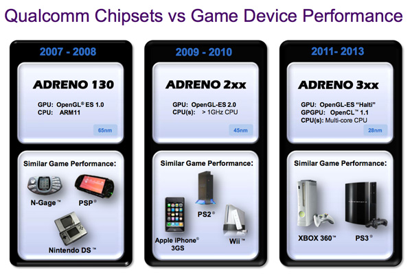
adreno3xx_sm.jpg


Since I recall another funky claim from IMG at xbitlabs mentioning something about PS3 performance (I just don't recall the exact claim and am too bored to dig it out), all falls into the same category. 2013 is a mighty long time from today. In 2012 NV should already be producing Tegra4. Different sides are just throwing around vague data about next generation devices. Only when they've all announced the specifics of each future architecture we'll get a tad wiser.

In any other case and until then we'll be reading about the Uber-T604, the Ultra-Adreno3xx, the Fantastic-Tegra3/4 and the Super-Series6 amongst others.

A far more important question would be what Uber-OGL_ES-Halti exactly stands for (what a stupid codename for an API anyway....).
 
As long as anybody doesn't fall for it, no harm done.
I'm sure there will be some that will fall for it.
http://www.anandtech.com/show/4024/...8960-28nm-dualcore-5x-performance-improvement

adreno3xx_sm.jpg


Since I recall another funky claim from IMG at xbitlabs mentioning something about PS3 performance (I just don't recall the exact claim and am too bored to dig it out), all falls into the same category. 2013 is a mighty long time from today. In 2012 NV should already be producing Tegra4. Different sides are just throwing around vague data about next generation devices. Only when they've all announced the specifics of each future architecture we'll get a tad wiser.

In any other case and until then we'll be reading about the Uber-T604, the Ultra-Adreno3xx, the Fantastic-Tegra3/4 and the Super-Series6 amongst others.
I know that all of them use roughly the same type of 'language' so on paper they all seem to be as good as the other cause they all have 'PS3 graphics performance', I wonder how good IRL they'll be.
A far more important question would be what Uber-OGL_ES-Halti exactly stands for (what a stupid codename for an API anyway....).
OpenGL 3.0 LITE?
 
I assume the '75% lower power' (i.e. 4x performance per watt) is relative to the original 65nm Snapdragon, not the 45nm shrink.

As for PS3/XBox360-level performance... What's the probability that any handheld chip has equivalent performance to a chip with 24 TMUs at 550MHz before 14nm in 2015? Zero.
(although in practice RSX's utilisation isn't mind-blowing, it's more optimised towards perf/mm2 than perf/unit, so I suppose equivalent performance on a ultra-high-end tablet chip on 20nm isn't strictly impossible).
 
Scorpion at 1.5GHz required the LPG process at 45nm. This is a significantly more power-hungry process than LP and far more so than 28LP. IIRC, 1.4W using a 1.5GHz LPG core and a 1.3GHz LP core. I'm going to make a rough, blind assumption that the LPG core consumes the majority of that; around 900mW-1W.

Seeing as this will likely run ~1.5GHz in 28LP and that you'd likely need ~1.0GHz or lower to match the performance of the previous 1.5GHz LPG Scorpion, having a new u-arch on 28LP that consumes ~300mW isn't out of the question.

But yes, this is with very fiddled numbers.
 
IIRC, 1.4W using a 1.5GHz LPG core and a 1.3GHz LP core. I'm going to make a rough, blind assumption that the LPG core consumes the majority of that; around 900mW-1W.
Ohhhhh. Wait, that chip uses two different synthesis jobs for the two cores, one of which uses only LP transistors and the other mostly G? I didn't know that, very intriguing. I thought the Marvell Armada 628 was the first to do something like that. This would also explain why Qualcomm is the only company that has invested in a dedicated DC/DC for each core; it would be problematic to share one DC/DC if the cores were rated for very different frequencies at a given voltage.

My assumption (if this is true) is that at very low frequencies the LP core takes significantly less power than the G core (which is therefore always power gated off in that case) due to lower leakage, but at the maximum frequency the G core takes *less* power than the LP core due to lower dynamic power. Anything else would be rather absurd and defy the whole point (with your numbers, you'd be better off with an overvolted LP core, that's insane!)

It's at times like this I feel like I really should finish that article on Icera one of these days! See slide 36: http://www.lirmm.fr/arith18/slides/ARITH18_keynote-Knowles.pdf :)
 
Back
Top