Well the Mac pro formfactor would necessitate reduced clocks compared to PC ethusiast being an AIO enclosed unit. If anything it's an indication that original leaks of 1500-1600 are probably accurate.We will need to see if the reduced clock speed (around 1350-1400MHz) is just for the Apple products or ends up the same with the Vega PC dGPU products.
Too early to say for now or just a limitation due to iMac Pro.
Cheers
Install the app
How to install the app on iOS
Follow along with the video below to see how to install our site as a web app on your home screen.
Note: This feature may not be available in some browsers.
You are using an out of date browser. It may not display this or other websites correctly.
You should upgrade or use an alternative browser.
You should upgrade or use an alternative browser.
AMD Vega 10, Vega 11, Vega 12 and Vega 20 Rumors and Discussion
Apple's iMac Pro page states 400 GB/s for the Vega GPU.
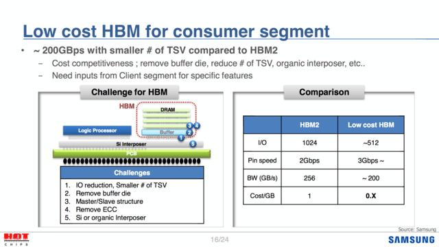
Vega GPU has Low Cost HBM by Samsung?

So Low Cost Samsung HBM2 has faster pin speed of 3 GB/s (+) that can deliver 200 GB/s compared to 256 GB/s on HBM2, 400 GB/s for 2 stacks configuration.
Vega GPU has Low Cost HBM by Samsung?

So Low Cost Samsung HBM2 has faster pin speed of 3 GB/s (+) that can deliver 200 GB/s compared to 256 GB/s on HBM2, 400 GB/s for 2 stacks configuration.
but vega has a 2048b bus for its memory configuration, the above is using 512 per stack, how does that work? Aren't teh Rops tied to the memory controllers now ?
Infinisearch
Veteran
IIRC thats a post HBM2 slide. Again IIRC its in parallel with HBM3.
iMacmatician
Regular
It seems a bit confusing to me.Probably a mistake in the video, in the event they said "over 400 GB/s"
- In 48:05-48:10 in the event video, the presenter says "over 400 gigabytes per second of memory bandwidth."
- The iMac Pro webpage has a description of the Radeon Pro Vega with "400 GB/s memory bandwidth."
- It is mentioned below the GPU diagram on that same page that "the GPU can fetch data at up to 400GB/s."
This confirms 48 ROPs. Either they are "uber" or great efficiency leap happened.
This confirms 48 ROPs. Either they are GREAT AGAIN or great efficiency leap happened.
Fixed it for you
I think the article posted afterwards mentions 64 ROPs?
http://wccftech.com/amd-debuts-rade...ailed-die-shot-22-tflops-400gbs-8-16-gb-hbm2/
iMacmatician
Regular
Where are the ROPs in the die picture?This confirms 48 ROPs. Either they are "uber" or great efficiency leap happened.
I'm not confident enough in my interpretation the diagram to be sure which block would be the ROPs, but it may still be 64 and consistent with the Linux patches.This confirms 48 ROPs. Either they are "uber" or great efficiency leap happened.
The CUs seem certain enough, although the way the shapes are divided might be consistent with a changed orientation. The CU is one long rectangle book-ended by a pair of rectangles towards the center and three rectangles towards the outside.
The rectangles further out seem to be one for every two CUs.
One possible interpretation:
The three rectangles in the CU are the L1, filtering, and l/s blocks, and this time they are not arranged along the center line of the chip. The outer rectangles above and below the CU arrays could be the shared front ends, this time shared between two CUs.
The RBE sections are the long bars on the right and left. The ROP sections seem to be more variable in layout, possibly to most efficiently pack them in the outer margins and around other miscellaneous units.
That would put the L2 as the two 8x3 arrays below the main portion of the GPU, and presumably above the blocks dedicated to the HBM interface and controllers.
The 8 columns in that case might pair up with the tile_pipe values listed in the Linux patches for Vega (the 8 marked with a ???). If the picture's 3 rows are accurate, that may mean a non-power of 2 associativity, or perhaps some other change.
The possible HBM interfaces have 12 columns each, although how much of that is in part due to oversimplifying some of the surrounding silicon around the PHY is uncertain.
The more pronounced spacing that cuts the CU arrays into 4 quadrants might be consistent with the need for connectivity to the L2 at the bottom for the changed layout of the CU caches and the ROPs on either side. Polaris' artistic rendition had a pronounced division along the center line, but that was before the DRAM and L2 was shunted off to one side and the ROPs hooked into the L2.
D
Deleted member 13524
Guest
No, you can't make TB3 controller out of PCIe lanes since it's not PCIe, but yes, they could support TB3 on Ryzen if they used separate Intel controller for it on the motherboard.
What I meant is you can implement a TB3 controller as long the CPU has enough PCIe lanes. The external TB3 controller will connect to the CPU through PCIe and not something else, right?

(DisplayPort connections seem to be just there as passthrough from a GPU, integrated or otherwise)
I'm just suggesting apple could have used Threadripper and connected one or more TB3 controllers to it, since the chip has an insane amount of PCIe 3.0 lanes.
Yes, that would have been possible.What I meant is you can implement a TB3 controller as long the CPU has enough PCIe lanes. The external TB3 controller will connect to the CPU through PCIe and not something else, right?
(DisplayPort connections seem to be just there as passthrough from a GPU, integrated or otherwise)
I'm just suggesting apple could have used Threadripper and connected one or more TB3 controllers to it, since the chip has an insane amount of PCIe 3.0 lanes.
ImSpartacus
Regular
VCZ has a "rumor" that AMD & Nvidia will both release cheaper crypto currency-optimized versions of their GPUs.
https://videocardz.com/70162/amd-and-nvidia-preparing-graphics-cards-for-cryptocurrency-mining
Considering how this topic was just being discussed on B3D (particularly a poignant post from Mr Ryan Smith), I'm wondering if this is a real rumor or just some feedback loop shenanigans.
I just don't think it's in AMD's (or Nvidia's) best interest to sell a cheaper crypto card. But if they can't find a way to gimp gaming cards, then maybe this is for the best.
EDIT It just dawned on me that I probably should've put this is that crypto thread...
Nvidia will really need to lower the price of the 1060 crypto mining version a fair amount to compete with AMD or Pascal higher GPU as its price/performance is not as great as the GTX1070 these days.VCZ has a "rumor" that AMD & Nvidia will both release cheaper crypto currency-optimized versions of their GPUs.
https://videocardz.com/70162/amd-and-nvidia-preparing-graphics-cards-for-cryptocurrency-mining
Considering how this topic was just being discussed on B3D (particularly a poignant post from Mr Ryan Smith), I'm wondering if this is a real rumor or just some feedback loop shenanigans.
I just don't think it's in AMD's (or Nvidia's) best interest to sell a cheaper crypto card. But if they can't find a way to gimp gaming cards, then maybe this is for the best.
EDIT It just dawned on me that I probably should've put this is that crypto thread...
From one of the crypto blogs:
.With prices for the GTX 1060 9Gbps not that much lower than the price of GTX 1070 there is actually not that much reason to go for it the faster memory instead of the faster GPU in general.
Personally with its efficiency I think they should also look at a cheaper mining specific 1070 as it has good performance relative to the 1060.
Cheers
It's proposal and HBM had 1024 IO pins just like HBM2Is that HBM2 or HBM? It seems to me it's uprated HBM (IO count ~same as HBM). But it also looks like a proposal, not a product.
Jawed
Legend
Why would AMD and NVidia be involved in this? It's the AIBs which take GPU chips from the IHVs and add all the gubbins required to make a card you can buy. It's also in their interest to offer a short warranty. And, it's also in their interest to sell cards that won't hit the second hand market as gamer cards.
Anarchist4000
Veteran
Have to ask for a source on this. Went through a dozen Nvidia pages and blogs and nothing official that I've come across states that. Just FP32/64 and Tensor. Emphasis on official and not a sites interpretation.Yes they did.
Same capabilities as GP100, so 30 TFLOPS for the Tesla V100
