AMD Bulldozer Core Patent Diagrams

from what generated the idea about speculative execution?

I read that this was only a first batch of info, when will amd release the others?
of what can they still talk about whitout giving intel the complete recipe?
 
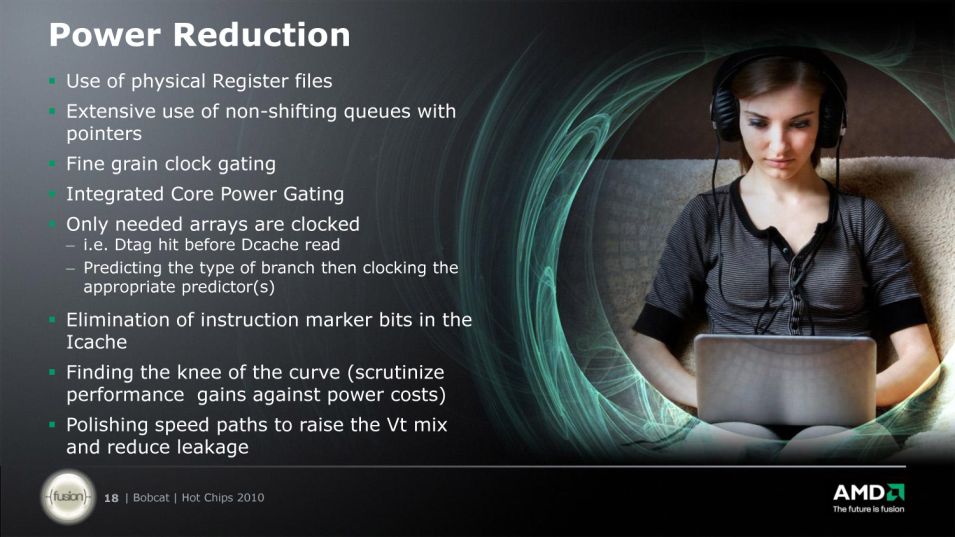
What do they mean by "Only needed arrays are clocked"?
BobcatHotChips_August24_8pmET_NDA-18_575px.jpg


I seem to recall some talk about unclocked execution a while back but I don't think I got it.
Are we talking like if 2 sequential stages actually take 0.75 clocks each, 3rd takes 0.5 clocks & a fourth takes the full clock, instead of taking 4 full clocks at one stage per clock, you might get your result in only 3 clocks by letting the result of each stage flow straight through to the next without having to pause till next clock?
 
from what generated the idea about speculative execution?
It probably came from a number of places, usually when people reviewed patent applications and presentations on similar ideas for architectures, such as AMD's patents and papers by Andy Glew. It's one of the perils of relying on patents and theoretical papers for predicting what a design will turn out to be.
Patents are not always used and architects are free to think up various ideas that may not come to fruition in a physical chip for any number of reasons, or may be deferred to later designs.
In addition to things like eager execution, Glew had posited a facility for extremely fast thread forking to the paired cores, amongst other things.

What do they mean by "Only needed arrays are clocked"?
Only so much of a cache is active in a cycle and arrays can be clock-gated when not in use.
The cache will wait for a hit to come back from the tag check before then selecting and powering the needed cache line. This adds latency to the process, whereas in most chips the arrays within the associative set begin the access process prior to knowing which line will actually be used.

There is the second line in that slide that seems to indicate there is slightly more indirection involved in branch prediction. My interpretation is that there is a branch predictor-predictor that will attempt to predict the branch type, and by extension only clock the type of predictor that is needed.
Given that branch history tables rival some small L1s in size and that there are now loop, jump, branch, indirect, and other predictors, this would save power at the price of likely worse latency.


The bulldozer slides indicate that there has been a change in the Int pipeline as well. The PRF-based register rename means its OoO scheme is likely closer to Bobcat's than K8 (which used reservation stations). This may make them closer in some ways to the Pentium 4 or K8's FPU.

The data cache is way-predicted. I'm not sure if K8 did this. P4 did, I believe.

Per-core, Bulldozer is slightly inferior in the number of load queue entries, and proportionately worse in store (40 vs 48, 24 vs 32)
However, in a multithreaded situation, the situation would change signficantly because most resources in the Intel solution are cut in half with threading, and then BD has a whole other core.

BD's branch predictor is capable of moving ahead of the main pipeline which in stall situations can keep the predictor's latency from adding to whatever stall happened in the main pipe.

There are more aggressive prefetchers, including a correlative prefetch for data accesses, which sounds vaguely like the application of a correlating branch predictor's methods to memory accesses.

Lightweight profiling is mentioned, and I'm curious about more details on that. It could be used by software to better load-balance or performance tune.
 
x86 CPU articles are getting harder and harder to read, as someone who likes dropping down to architectural optimizations its littered with my screams when reading all these optional and conflicting extensions.
x87 and SSE2,
~8 partially conflicting version of SSExy,
now AVX which tries to fix alot of this... by introducing yet another coding scheme...
and FMA4/FMA3 differences is already the first crutch in AVX before any CPU is released.

Moore`s law surely can be extended to x86 Software - if you want to optimally support x86 CPUS, your codepaths will double every few years.
 
Only so much of a cache is active in a cycle and arrays can be clock-gated when not in use.
Oh yeah that is a power management slide :oops: clocked as in powered up, unused bits powered down.
 
It probably came from a number of places, usually when people reviewed patent applications and presentations on similar ideas for architectures, such as AMD's patents and papers by Andy Glew. It's one of the perils of relying on patents and theoretical papers for predicting what a design will turn out to be.
Patents are not always used and architects are free to think up various ideas that may not come to fruition in a physical chip for any number of reasons, or may be deferred to later designs.
In addition to things like eager execution, Glew had posited a facility for extremely fast thread forking to the paired cores, amongst other things.

He describes his idea here. He investigated fork-on-call, where state is duplicated whenever a CALL instruction is encountered, executing both the call-target and, speculatively, the code after the CALL. This requires a fast way to duplicate state and a log to subsequently merge state.


Cheers
 
One hardware thread can only execute on one or the other of the integer units.

Yep but I don't really see how Bulldozer's setup prevents the dispatch of instructions from one thread to both integer blocks in parallel. The fetch/decode logic is shared so where does the limitation come from? I wouldn't be surprised at all if this is in fact possible and it's marketed as running one thread on two "cores" or some similiar nonsense :) Or is it not possible cause the L1's are independent?
 
Yep but I don't really see how Bulldozer's setup prevents the dispatch of instructions from one thread to both integer blocks in parallel. The fetch/decode logic is shared so where does the limitation come from? I wouldn't be surprised at all if this is in fact possible and it's marketed as running one thread on two "cores" or some similiar nonsense :) Or is it not possible cause the L1's are independent?

It has several issues, like pushing data across reg files, not to mention L1 of the other core is unlikely to have any data that the migrating thread might need.
 
Yep but I don't really see how Bulldozer's setup prevents the dispatch of instructions from one thread to both integer blocks in parallel.
As already noted, L1 is private to a hardware thread.

The fetch/decode logic is shared so where does the limitation come from?
The data handled by the shared logic is vertically 2-way threaded, i.e. there are separate resources for each thread. The shared logic runs in stages that are decoupled from each other, with queues from one to the next stage. This provides flexibility/latency-hiding. Pretty much like the queues you see between the stages in a graphics pipeline.

What will be interesting is what happens when two very heavy threads are running, both with plenty of ILP - looks like a good way of swamping the front-end. There might be recompense if both threads are running the same loop from the same program - but then again...

x86 isn't my subject at all.
 
Yep but I don't really see how Bulldozer's setup prevents the dispatch of instructions from one thread to both integer blocks in parallel. The fetch/decode logic is shared so where does the limitation come from? I wouldn't be surprised at all if this is in fact possible and it's marketed as running one thread on two "cores" or some similiar nonsense :) Or is it not possible cause the L1's are independent?

Unless the processor state is shared between cores, there would be discrepancies that could lead to anomalous execution.
Each core would need to be in sych with regards to data, flags, modes, and exception handling. That means the retirement logic, flags, register files, store queues, and forwarding would need to be updated with common values.
If these were merely integer clusters without separate schedulers and instruction control units, this would be feasible.

As described so far, these would not be shared. Results would not be forwarded between cores, and one core could not forward from the store queues of the other. That could lead to markedly different execution behavior dependent on the exact state and distribution of instructions that x86 should not permit (load should have hit a store on the other core, instead loads from its own L1, should have gotten a forwarded result, does not have the right rename register, etc.).
Unless the retirement logic in one core is able to signal the other, one core could hit a mispredict or exception, and the other could retire instructions it should not have.

If the front-end knew more about what it was decoding it could steer things around such problems, but at that point it is taking on more of a central role in instruction control and the "cores" would not be cores. The descriptions do not attribute that level of complexity to the centralized resources.

Without more data, it does not look like the core pipeline has changed so radically as to allow this level of sharing.
 
Yep but I don't really see how Bulldozer's setup prevents the dispatch of instructions from one thread to both integer blocks in parallel. The fetch/decode logic is shared so where does the limitation come from? I wouldn't be surprised at all if this is in fact possible and it's marketed as running one thread on two "cores" or some similiar nonsense :) Or is it not possible cause the L1's are independent?

The first problem to solve for speculative branching in principle is that of not invalidating speculated resources. Look at this:

a = b + c;
if (a <0)
write a to 0x010
else
write a to 0x100

Either branch just contains a write-to-memory. If you execute both you would start modifying the contents of two locations in the memory-hierarchy, which you can not take back. At least not without a transactional memory-hierarchy, which has roll-back (not even Ultra-SPARC future had that). At least the two locations are seperate, but here:

a = b + c;
if (a <0)
write 0x010 -= a
else
write 0x010 += a

We start to have concurrent conflicts within the upper memory-hierarchy (caches) and the write-back queues. So for speculation you'd have to carry an enourmous amount of duplicated resources with you (or mark cache-lines as "clones", means having multiple alternate versions of the same adress).

As you see in the example it's absolute inefficient to speculate (the example), saving 4 clocks misprediction penalty for say 240 clocks internal rollback, double cache occupation and 15% more transistor logic.

The comes the question branch-in-branch ... how much resources do you want to throw at it before you allow it stalling? The lashback post-stall for cleaning up (all destructive modified resources) is proportional to the utilized resources.

If'd we use our second core in BD we have to make a little bit less and a little bit more. The instruction decoder effectively has tu de-interleave the instruction stream, simulating to the first core as if we have a continous branch-free left branch and the right to the other (including duplication of the register-file etc., everything which defined a current state in a program). Additionally we need some frontend-logic which evaluates the branch-condition itself (needs it's own ALU, AGU, load-port, etc. a mini-core). All in-core can more or less stay the same. On the backend we'd then need some merger-logic which simply says which core is at fault and throw away (or roll-back) any changes to the memory-hierarchy; would be easier with transactional-memory.

You see, then the front-end needs something like 2000 clocks to make core 1 and 2 state-identical, you still have double cache occupation and 5% more transistor logic and a real mess in the layout because you have to route the register-file to register-file bus.

So on the first glance it's not really faster is it? ;) All that just for a one-line write-switch which isn't a serious problem?

If you really want to go into it, and get some smart ideas (unified register-file fe.), then it probably will converge in a working solution ... but that's another architecture then, not BD as-is.
 
No AM3 compatibility

I think AMD has just pulled another socket 939 fiasco. AM3 motherboards won't accept Bulldozer.
http://www.planet3dnow.de/cgi-bin/newspub/viewnews.cgi?category=1&id=1282840508

When we initially set out on the path to Bulldozer we were hoping for AM3 compatibility, but further along the process we realized that we had a choice to make based on some of the features that we wanted to bring with Bulldozer. We could either provide AM3 support and lose some of the capabilities of the new Bulldozer architecture or, we could choose the AM3+ socket which would allow the Bulldozer-base Zambezi to have greater performance and capability.

The majority of the computer buying public will not upgrade their processors, but enthusiasts do. When we did the analysis it was clear that the customers who were most likely to upgrade an AM3 motherboard to a Bulldozer would want the features and capability that would only be delivered in the new AM3+ sockets. A classic Catch-22.
AMD should have launched AM3+ with Thuban. They've really fucked that up.
 
AMD should have launched AM3+ with Thuban. They've really fucked that up.

But wouldn't that have just been crapping on AM3 owners? At least the way things are, AM3 owners (the vast vast, vast, vast majority of whom won't have bought an AM3 board just for Thuban) still have an upgrade path to some pretty damn fast 6 core processors.

I'm still rocking a 939 system and playing games on it. I don't see this as being as bad as what happened to us - fast 939 dual cores (with 2MB of L2) were dropped faster than you can say "fuck 939 owners" and then went for approximately $infinity on ebay.

What I want to know is when are AM3+ boards will be available. I've held off upgrading specifically because I wasn't sure that AM3 would support Bulldozer.
 
We still have to know the exact capability which supposly would be crippled by using AM3 ... tri-channel, ECC, additional HT-links ... they are all gracefull-degradable features. Maybe power-gating needs a specific electric infrastructure?

A CPU designed for >AM3+ also seems uh, contradicting the entire twoway-compatibility AM+-socket concept. Better name it FU1.
 
But wouldn't that have just been crapping on AM3 owners?
No, because AM3 processors work in the AM3+ socket. Thuban should have been AM3 to go in a newly launched AM3+ socket.

I'm still rocking a 939 system and playing games on it. I don't see this as being as bad as what happened to us - fast 939 dual cores (with 2MB of L2) were dropped faster than you can say "fuck 939 owners" and then went for approximately $infinity on ebay.
My S939 X2 3800+ sounds slower than yours. I have AGP too: X1950Pro hanging in there.

What I want to know is when are AM3+ boards will be available. I've held off upgrading specifically because I wasn't sure that AM3 would support Bulldozer.
Precisely.
 
Dumb question.
In many places I found the statement that (when using the SIMD units) that Sandy bridge has twice the throughput of Bulldozer, they are comparing two "sandy bridge cores" to a Bulldozer "module" right?
 
Dumb question.
In many places I found the statement that (when using the SIMD units) that Sandy bridge has twice the throughput of Bulldozer, they are comparing two "sandy bridge cores" to a Bulldozer "module" right?

Yes. 1 SB core ~2x the fp rate of 1 BD core.
 
Back
Top