A Preview of PSP motherboard(Clie motherboard)

pda25_03.jpg

pda25_04.jpg

pda25_05.jpg

pda25_06.jpg

pda25_07.jpg

pda25_08.jpg

pda25_09.jpg
 
nice find , not only that but the first picture gives us an idea of the size and shape of the handheld .
 
Seeing the actual thing will impress you a lot more than the pictures, I have seen the real thing and I think it looks great and is extremely compact.
 
*scratches head*

ok, this being a clie ux series board relates to the psp how?

*keeps scratching head*
 
...

cli04.jpg

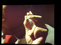
Purhaps we can estimate the handheld engine die size from this pic. This will be a good indicator of PSP chip size.

Gee, the Handheld Engine appears to be in excess of 200 mm2, purhaps approaching 300 mm2.
 
Gee, the Handheld Engine appears to be in excess of 200 mm2, purhaps approaching 300 mm2.

From the old maskrider post

0.18u, 64Mbit eDRAM, core <-> memory 4x128bit bus connection, running Palm OS 5.2, Dynamic Voltage and Frequency Management (8-123MHz, core 1.2-1.6V, I/O 2.5-3.3V, standby 1.7mW, MPEG-4 playback around 270mW).

Its no suprise if it is big ;)
 
Re: ...

DeadmeatGA said:
Gee, the Handheld Engine appears to be in excess of 200 mm2, purhaps approaching 300 mm2.

You're not natively metric are ya? I'd be rather surprised if that thing is even 200sqmm. 300's totally out of the question unless that dude has like the world's biggest hands.

*G*
 
I'd be rather surprised if that thing is even 200sqmm.
It already exceeds 200 mm2. The HE is as wide as that dude's finger holding it. Do the math and you can estimate the die size. This is the only way since there is no officially published die size info.

300's totally out of the question unless that dude has like the world's biggest hands.
I am not so sure. My finger measures 20 mm wide.

Let's do some number crunching

14 mm x 14 mm = 196 mm2
15 mm x 15 mm = 225 mm2
16 mm x 16 mm = 256 mm2
17 mm x 17 mm = 289 mm2

PSX2 on a chip taken as base, the PSP chip on 90 nm is guaranteed to be signifantly larger than PSX2OAC because it has slightly more logic transistors(Twin CPUs, an audio DSP) while the eDRAM gate count trippled(4 MB Vs 12 MB).

Apparantly, Sony is the only vender in the world that puts 200+ mm2 chips in handhelds.

Things doesn't look good for CELL, since it is quite clear that they are bound by same law of fabrication as everyone else. A 4-core CELL in PSX3?? Forget it.
 
Did you just deduced things will not be looking good for CELL based on the Sony Clie's chips ?

I would have not expected this form you... :LOL:
 
DeadmeatGA said:
It already exceeds 200 mm2. The HE is as wide as that dude's finger holding it.

1: One of the fingers obscures part of the chip. 2: the chip is held at an angle compared to the camera. 3: the pic is small. 4: you can't guess much of anything re. the chip size without a fixed frame of reference, and a pair of (probably japanese, hence likely small) hands isn't going to be it.

Still, all this never stopped you from speculating before, so why expect it would do so now? :/

Do the math and you can estimate the die size.

No thank you.

Let's do some number crunching

Deadmeat-style number crunching to determine H-E die size:

Retrieve irrelevant baseline (PS2 EE+GS die), add imaginary constant, multiply by made-up factor, finally round upwards using DMGA guesstimate algorithm to come up with "fact" that Cell cannot possibly for any reason consist of four PEs despite being built on entirely different CMOS process and having nothing in common with any of previously mentioned chips.

Done!


There IS NO SUCH THING! It's PS2, ya maroon. It even says so silkscreened to the top cover of the console, open your friggin eyes man.


*G*
 
...

1: One of the fingers obscures part of the chip.
Irrelevant. We are not looking for the details of chip, but the length and width of this chip so that we can estimate the die size.

2: the chip is held at an angle compared to the camera.
Irrelevant. The ratio of chip width & height to the finger remains the same.

3: the pic is small.
Blow it up.

a pair of (probably japanese, hence likely small) hands isn't going to be it.
1. A Japanese hand(especially that of adult male) is not that small.
2. You can clearly observe two references of chip height from that picture.
A. The HE is as tall as the thumb nail.
B. The HE is as tall as the width of middle finger holding it.

Do your calculation either way, you still get the same result exceeding 200 mm2. The HE is one massive chip(By chip fabrication standard), despite having an ARM9 core and 8 MB of eDRAM. Now imgaine how large a PSP chip with twin R4000s, one Vector FPU, twin GPUs, a DSP, a variety of I/O controllers, and 12 MB of eDRAM will be.
 
Re: ...

DeadmeatGA said:
The HE is one massive chip(By chip fabrication standard), despite having an ARM9 core and 8 MB of eDRAM. Now imgaine how large a PSP chip with twin R4000s, one Vector FPU, twin GPUs, a DSP, a variety of I/O controllers, and 12 MB of eDRAM will be.

as originally submitted by maskrider (and kindly brought up by v3), the HE is one massive chip integrating an ARM9 core, 8MB RAM and a DSP, all that produced on 180nm tech. i think it's quite reasonable for its die to be in the ~200s of square mm. btw, if you sometime care to open your cell phone you may be surprised to find some pretty chunky ICs there, too (usually two - a cellular digital transciever and a "cpu" core incorporating flash, ram, etc).
 
...

the HE is one massive chip integrating an ARM9 core, 8MB RAM and a DSP, all that produced on 180nm tech. i think it's quite reasonable for its die to be in the ~200s of square mm.
If you moved the HE to 90 nm process, then its die would measure in 50~60 mm2. But PSP will have at least 4 times the logic and 50% more eDRAM, so the net sum is about equal. In other word, the PSP chip is going to be hugh(But not by Kutaragi Ken's standard anyway, he doesn't mind putting 280 mm2 chips into consoles).
 
Back
Top