Nvidia Blackwell Architecture Speculation

  • Thread starter Deleted member 2197
  • Start date
My guess is that the outer yellow one is the I/O daughterboard mezzanine connector, and the green one is for the PCIe Gen5 daugtherboard. Could be vice versa but this seems to make it easier to route the ribbon cables.
View attachment 12807View attachment 12808

NVIDIA's Unreleased TITAN/Ti Prototype Cooler & PCB | Thermals, Acoustics, Tear-Down. A similar mezzanine connector for the PCIe daughterboard on the prototype RTX 4090 PCB, courtesy of GamersNexus

View attachment 12809
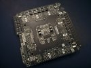
Ggz06G4WAAAt0kt.jpg
Actual photo of the back of the main PCB. I'm curious about the acoustic performance of the new miniature chokes and whether they'll produce coil whine.


5090 FE Design Discussion with Justin Walker, Nvidia Sr. Director of Products
 
So, GB202 has 128 MByte L2-Cache, if I'm interpreting the 8 x 16 MByte partitions in that picture correctly. Forgive me, but the search has not come up with anything regarding L2 size except rumors from a year ago.

Image taken from Nvidias Website.
 

Attachments

  • nvidia-blackwell-die-shot.png
    nvidia-blackwell-die-shot.png
    863.2 KB · Views: 26
To be fair, FP4 is now widely used in LLM inference. 40-series does support INT4 but it's not very useful. Of course, comparision between FP4 and FP16 is probably not a good sport, but AFAIK people has found that using FP4 with twice as many parameters generally perform better than FP8 (the same goes to using FP8 with twice many parameters compared to FP16), so generally it'd be preferable to use FP4 if a larger model is available.
 
Do we know if the RTX 50 series still have the hardware optical flow accelerators, and if so, whether they serve any purpose for regular consumers or are just dead silicon?
They'll still exist, they just wont be used for any special graphics features this time round, outside potentially for fallback if DLSS3 framegen gets used instead of the new DLSS4 model.
 
That list disregards any architectural changes between families and as such is just as misleading as anything else.
Do you really expect significant architectural gains in like for like work other than the support for things like FP4? I certainly don't and the performance numbers provided certainly don't suggest a massive improvement in architecture..... If we can find a 4000 series card that's close enough in specs to a 5000 series variant and then compare them at the same clock speeds in like for like work, I don't think we'll see a massive improvement at all.
 
@RobertR1 The design opens up a lot of cooling options, especially if you have a creative case with a riser cable. I've always hated that cards have fans that force air onto the card pcb which ends up blowing air out the sides of the card, which them blows onto the side of your case and onto your motherboard.
 
There's a reason for Jensen saying this. But I think he should have said it in a more straightforward way. For example in Blackwell, INT32-throughput per SM has doubled.
Nice! I assume there are some new docs being sent out?
Still the official specs on the website suggest that FP32/INT32 ratio hasn't changed. So FP32 doubled as well? Did they go with 32-wide SIMDs and got rid of 2-cycle launch cadence?
 
brilliant

Ah it's already posted but yeah I'm in awe of this. If it actually delivers good cooling performance at 600w, then it's on a different level.
That's just the usual pass thru cooling right? A bliss for cases like fractal ridge, but a nightmare for sandwich cases like nr200p
 
Nice! I assume there are some new docs being sent out?
Still the official specs on the website suggest that FP32/INT32 ratio hasn't changed. So FP32 doubled as well? Did they go with 32-wide SIMDs and got rid of 2-cycle launch cadence?
I don't know of any new docs. FP32 does not need to double - and I am not aware of such a thing. But in Ada, only one of each SIMD16 pairs was combined INT32/FP32, the other one was FP32-only.
 
Not sure if this will have some insights in terms of Blackwell's potential configuration once more information comes out.

The 5090D was launched in China with the only difference being 2/3 the AI TOPs spec. CUDA core specs and RT TFLOPs is listed as identical to the 5090, so it suggests the chip is not cut at the SM level or clock speeds. Not sure if any Nvidia GPU has been cut at the sub SM (or really TPC) level before? The 4090D was cut at the SM/TPC level to comply, and therefore proportionally lost specs across the board.

Could just be artificially limited via firmware and/or drivers. Not sure off hand what the language is in the GPU restrictions and whether it would allow for that.
 
Back
Top