The Intel Execution in [2024]

Status
Not open for further replies.
It was pretty bad with Alchemist even discounting for the several major driver updates fixing loads of stuff.

Also 272mm2 N5 die. This is close to AD103 (!), can't imagine it bringing any margins for them.

They need to launch solid. Hopefully they learned a lot of lessons and this one comes out in a much better state. Alchemist looked pretty decent after all the major updates.
 
It was pretty bad with Alchemist even discounting for the several major driver updates fixing loads of stuff.

Also 272mm2 N5 die. This is close to AD103 (!), can't imagine it bringing any margins for them.
Where was die size & process mentioned? Didn't notice in press materials.

I think you're painting far worse image of the driver reality of today, early days for sure but not today
 
As independent subsidiary, not separate division.

Whatever the terminology, still a part of Intel but with earnings reported separately as I mentioned.

If this card lives up to the promises it's a really nice deal. $250 for a better than 4060 with all of the features like ray tracing, frame gen, AV1. Exactly what the industry needs. Competition at the affordable price points. I'm not going to congratulate intel until it's been tested, but so far so good.

Also 12/10 GB of VRAM which is a good step up from 8 GB. If the 5060 sticks to 8 GB which as per the rumours it will, this is a decent alternative.

It was pretty bad with Alchemist even discounting for the several major driver updates fixing loads of stuff.

Also 272mm2 N5 die. This is close to AD103 (!), can't imagine it bringing any margins for them.

I presume you meant AD104 which is ~294 mm2. AD103 is ~379 mm2. It's not the most area efficient for sure but it's not as bad as Alchemist. And power efficiency is not bad either.
 
Where was die size & process mentioned? Didn't notice in press materials.
GN video:

I think you're painting far worse image of the driver reality of today, early days for sure but not today
It is pretty bad today, was close to unusable back at launch. So they have improved but it is still bad. Most recent releases show A-series underperforming rather heavily despite them using DX12 and sometimes RT.

I presume you meant AD104 which is ~294 mm2.
Yes, sorry, a typo. Still puts the new B580 in the same complexity territory as a 4070Ti.
 
Last edited:
It is pretty bad today, was close to unusable back at launch. So they have improved but it is still bad. Most recent releases show A-series underperforming rather heavily despite them using DX12 and sometimes RT.

Is that a driver problem though? Alchemist is just slow at certain things that probably can't be fixed with drivers.

B580 will be a nice card if it can consistently beat the 4060 for $250. At least until Nvidia and AMD show their hand in the $300 segment.
 
Yes, sorry, a typo. Still puts the new B580 in the same complexity territory as a 4070Ti.

So I just came across additional details.

Intel BMG-G21
- TSMC N5
- 272 mm²
- 19,6 Billion Transistors
- 72,1 MTr/mm²

This is pretty poor density. AD107 as per TPU is 18.9B transistors with a 159mm2 die size. And this barely beats AD107. Intel are definitely not making much of a margin on this, esp with the additional 4 GB VRAM. No direct comparison to AMD since they don't have mainstream N5 parts but N33 is 204mm2 on N6 and is fairly close in performance.
 
This is pretty poor density. AD107 as per TPU is 18.9B transistors with a 159mm2 die size. And this barely beats AD107.
Do we know how they compare in caches? Could be that Intel's chip has less of those but more logic?
If these would be equal between them and we'd disregard the density/size issue then competing on the same transistor complexity with a 100% similar feature set would actually look pretty good for Intel.
But I feel like Nvidia has traded logic for cache on AD107 so they are getting more out of less execution units - and is also why the chip is so much smaller probably?

So as per TPU, AD107 has 32MB of L2 and from the GN video, G21 has 18 MB. There is also a 192 bit vs 128 bit interface and Intel seems to have a larger media block as it supports AV1 decode and newer display outputs. There also might be a small difference in process as Intel states they are using the TSMC N5 process. Not sure if they literally mean N5 or the N5 family as Nvidia is using 4N which is a slightly denser variant. All of these factors should contribute a bit towards lower density, but even taking them into account, Intel appears to have a fundamental difference/drawback in physical design and the density shouldn't be this low vs the competition. GB207 and N44 should easily beat it while being significantly smaller.
 
could it be that the transistor numbers reported are just the functional ones while the chip area actually allows and includes a 256 bit mem controller with some units disabled as per techpowerup preview suggests "The 5 Render Slices and 20 Xe cores talk to each other over a next-generation global dispatch unit, and an 18 MB L2 cache. The GPU features a 192-bit GDDR6 memory interface. The odd count of 5 slices and 192-bit memory bus suggests that the BMG-G21 features a sixth render slice and a wider 256-bit interface, but that will probably be used in a higher SKU in the near future."
 
Memory interfaces, especially the PHYs, have also been the worst scaling structures with process node progression.

So on the consumer side those wider memory interfaces tend to be preferred from a VRAM (and to some extent higher relative performance in certain scenarios like higher resolutions) standpoint but they're relatively costly in terms of the die and and power cost stand point compared to being able to extract the performance and the ability to feed it via other means.

Intel seems to have a larger media block as it supports AV1 decode and newer display outputs

DP 2.1 functionality but AV1 encode and decode is present on AD chips as well. Although maybe the encoder and decoder support more features?
 
could it be that the transistor numbers reported are just the functional ones while the chip area actually allows and includes a 256 bit mem controller with some units disabled as per techpowerup preview suggests "The 5 Render Slices and 20 Xe cores talk to each other over a next-generation global dispatch unit, and an 18 MB L2 cache. The GPU features a 192-bit GDDR6 memory interface. The odd count of 5 slices and 192-bit memory bus suggests that the BMG-G21 features a sixth render slice and a wider 256-bit interface, but that will probably be used in a higher SKU in the near future."

Seems unlikely, that's just speculation. They already have a salvage part in the B570 and you don't need a 256 bit bus for this level of performance really. There is a rumoured G31 coming next year with 32 Xe cores and a 256 bit interface but judging by G21's performance, it would be around 4070 levels at best.

Memory interfaces, especially the PHYs, have also been the worst scaling structures with process node progression.

So on the consumer side those wider memory interfaces tend to be preferred from a VRAM (and to some extent higher relative performance in certain scenarios like higher resolutions) standpoint but they're relatively costly in terms of the die and and power cost stand point compared to being able to extract the performance and the ability to feed it via other means.


DP 2.1 functionality but AV1 encode and decode is present on AD chips as well. Although maybe the encoder and decoder support more features?

Yep exactly that's what I mentioned, the 192 bit interface will certainly have an effect on the overall density vs AD107.

Perhaps, could be higher resolution/bitrate support but I wasn't able to find concrete info to compare. But it will be a marginal difference. Overall I was saying that even considering all the factors, the density is still quite low in comparison. It has almost the same density as N33 on TSMC N6 despite a full node advantage. The similarly sized AD104 on a similar node is ~121M transistors/mm2 in comparison, almost 70% higher.

Edit: Battlemage also apparently was designed with PCIE 5.0 but it wasn't productized -
 
Last edited:
Intel is considering outsiders for the next CEO.

On anothet note, Pat has previously stated the recruitment from NVIDIA is very difficult.

Jensen has created a horizontal management structure that eschews a traditional hierarchy, making it almost impossible to identify who among them might be best positioned to take a step up — at Nvidia or at another company.


A flat organization is the best model I've ever worked under. We basically didn't have two or three layers of management that most other groups would. Great experience.
 
Celestial/Xe3 hardwarewise pretty much done, hardware teams now working on Druid/Xe4

The way I would like to comment is our IP that's kind of called Xe3, which is the one after Xe2, that's pretty much baked, right. And so the software teams have a lot of work to do on Xe3. The hardware teams are off on the next thing, right. That's our cadence, that we need to keep going.

 
A Korean outfit is reporting a 10% yield on 18A. Oof!

Yeah, except that it's not even supposed to be anywhere near ready yet, they're supposed to ship first samples sometime during H1/25 and start ramping to mass production in H2/25.
They're just making headlines for clicks, Intel being already down makes it juicy regardless of if there's any actual meat on the bones.
 
Why does anybody pay attention when any of these "news" outlets mention "yields". What yields? For which parts?

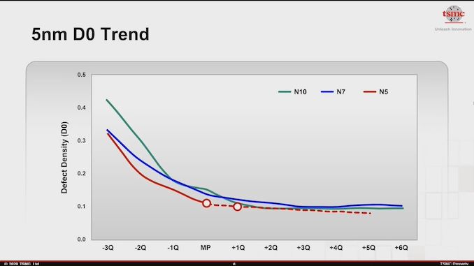
Intel has publicly mentioned that the D0 for 18A is under 0.4, and at that point it was like a year to mass production. For comparison for TSMC, D0 for N5 and N7 was ~0.3-0.35 at 3Q before mass production.

Manufacturing%20Excellence.mkv_snapshot_02.11_%5B2020.08.25_14.16.22%5D_575px.jpg
 
Status
Not open for further replies.
Back
Top