AMD Vega 10, Vega 11, Vega 12 and Vega 20 Rumors and Discussion

AMD has since updated their announcement, confirming that there isn't any on-package memory after all. The chip has a 256-bit GDDR5 memory controller, with the Chinese console shipping with 8GB of the stuff.

As for the die, I agree it sounds like it's a monolithic die due to the presence of GDDR5. However I'm not hedging my bets until AMD confirms it or we get pictures. New dies aren't cheap, even on the now tried and true 16nm process.

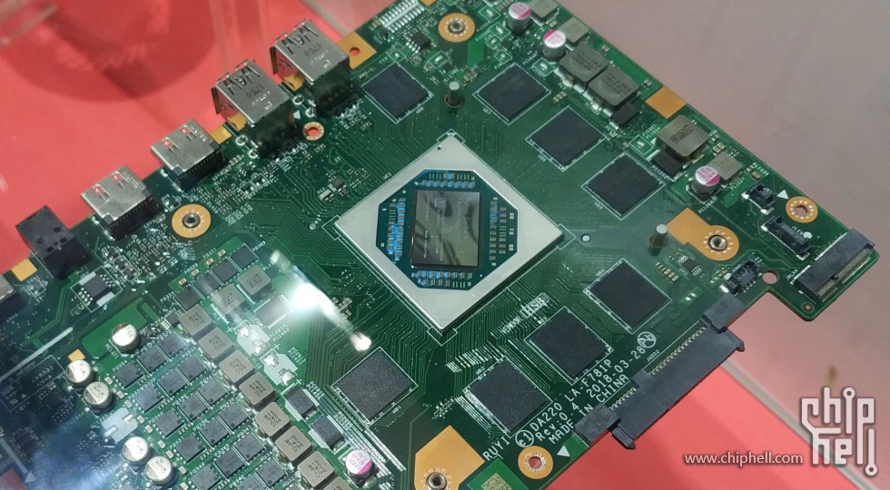
So this is TSMC, not GloFo? Off-package GDDR5 makes sense, as I don't see what having it on package would achieve, apart from making said package huge.
 
183507ya075aee67bbffk6.jpg


The photo isn't clear enough to make out who may have fabbed it. But it does make it clear that it's a monolithic die. So someone put down some pretty pennies for this...

So this is TSMC, not GloFo? Off-package GDDR5 makes sense, as I don't see what having it on package would achieve, apart from making said package huge.
All semi-custom to date has been TSMC. I certainly wouldn't expect this to be any different, especially with the geopolitical issues at hand.
 
I think probability is pretty high this is really a Vega chip. With the announcement saying it's a SoC, (KBL-G isn't), so it's really a new chip. And, gpu clock is 1.3Ghz. While this is doable with Polaris it definitely isn't something you want to do in such an APU (as the power draw goes through the roof for little gain). There were rumors of "Fenghuang Raven" since ages, so I guess it indeed materializes...
Keep in mind that would theoretically be a TSMC fabbed Polaris so the clock profile might be different and 1.3GHz more reasonable. I'd agree it's more likely Vega as RPM in that market would be significant where image quality is less of an issue. This looks to be a Chinese ESports platform or a distributed mining network in the making.
 
183507ya075aee67bbffk6.jpg


The photo isn't clear enough to make out who may have fabbed it. But it does make it clear that it's a monolithic die. So someone put down some pretty pennies for this...

All semi-custom to date has been TSMC. I certainly wouldn't expect this to be any different, especially with the geopolitical issues at hand.
This die looks huge.
 
Maybe big, but I wouln't call it huge. The die size seems to be very comparable to Scorpio Engine or XBox One SoC.
 
    • VK_KHR_create_renderpass2
      • This extension provides a new entry point to create render passes in a way that can be easily extended by other extensions through the substructures of render pass creation.
    • EXT_vertex_attribute_divisor
      • This extension allows instance-rate vertex attributes to be repeated for certain number of instances instead of advancing for every instance when instanced rendering is enabled.
  • https://videocardz.com/driver/amd-radeon-adrenalin-edition-18-8-1-beta
Primitive shaders?
 
2Gbps HBM2 is now in a shipping graphics card.

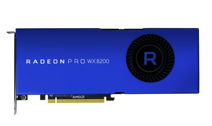
RadeonProWX8200_Straighton_RGB_XL_5inch_678x452.jpg


https://www.anandtech.com/show/13210/amd-announces-radeon-pro-wx-8200

At a high level this is another 8GB Vega 10-based card, using 2 stacks of 4-Hi HBM2 memory, and creating an important product distinction between the WX 8200 and the WX 9100, as the faster card remains the only modern Radeon Pro WX card with 16GB of VRAM. However the memory clock on the WX 8200 is quite curious: it’s not 1.89Gbps like every other full-speed Vega 10 card we’ve seen to date, but rather runs at a flat 2.0Gbps. The end result is that the WX 8200 actually has the greatest memory bandwidth of any Vega 10 card, with 512GB/sec of memory bandwidth. And consequently, there are going to be edge cases where the WX 8200 is actually faster than the WX 9100 – particularly raw pixel throughput-bound scenarios – as the new card enjoys a small memory clockspeed advantage.

AMD for their part isn’t drawing a whole lot of attention to the matter. But when poked about it, they’re mentioning that the WX 8200 is using SK Hynix’s “Gen 2” HBM2, which unveiled earlier this year, offers memory speeds up to 2.4Gbps. The net result of this is all of a 6% increase in memory bandwidth – so don’t expect to see AMD replacing existing products for slightly faster memory – but from a tech perspective it’s an accomplishment for AMD that, at last, they’ve finally hit 512GB/sec of memory bandwidth on a Vega 10 part, just as they originally wanted to.

So SK Hynix's 2nd gen 2Gbps and 2.4Gbps HBM2 is far enough along to ship (or at least the 2Gbps stuff is).
 
New set of Vega20 patches:

https://lists.freedesktop.org/archives/amd-gfx/2018-August/025239.html
https://cgit.freedesktop.org/~agd5f/linux/log/?h=vega20_psp_smu

Interesting things found so far:

SMU11 brings XGMI link support:

Code:
#define NUM_XGMI_LEVELS 2

#define MAX_XGMI_LEVEL (NUM_XGMI_LEVELS - 1)

uint8_t XgmiLinkSpeed [NUM_XGMI_LEVELS];
uint8_t XgmiLinkWidth [NUM_XGMI_LEVELS];
uint16_t XgmiFclkFreq [NUM_XGMI_LEVELS];
uint16_t XgmiUclkFreq [NUM_XGMI_LEVELS];
uint16_t XgmiSocclkFreq [NUM_XGMI_LEVELS];
uint16_t XgmiSocVoltage [NUM_XGMI_LEVELS];

Another check-mark for the leak from over a year ago.
 
I believe Raven Ridge H APUs are ~35W mobile SKUs. Maybe they will be based on newer silicon revision, which will improve energy efficiency. It is also possible that they'll be moved to 12nm lines, but I expected, than 12nm process will be used for the next generation Picasso APU (Raven Ridge shrink).
 
Back
Top