Haswell vs Kaveri

Has anyone seen a review that compares the A10-7850k IGP with a HD7750 GDDR5/DDR3?

The results are just proof of the Pink Elephant in the Room: lack of memory bandwidth.

The only balanced solution is the A8 with 6 GCN CUs and a 45W TDP.
Above that, increasing the available power and number of CUs is worthless.

And why is there no comment from anandtech or anyone else about the presence of two 128-bit memory controllers in Kaveri?


On the other hand, imagine a native 8 core, 16 thread Haswell with 16MB L3 and no IGP and 150W TDP :oops:

You mean a LGA-2011 Haswell? They should be coming later this year.
 
So basically, there are some nice improvement for 45W chips, especially but not only on the GPU side, and it bodes quite well for mobile SKUs, but Kaveri is essentially pointless at 65W or more. I guess that's it, AMD is definitely out of the enthusiast desktop market. Oh, well.
The 45W comparisons seem to be a bit misleading though because the old 45W 6700T typically has a power consumption ~10W lower than the 45W a8-7600. (I guess it's possible the 6700T can reach the same power use but it it looks like it usually doesn't). Never mind the anemic a8-6500t amd apparently wanted to get used for comparisons :).
Still it looks like some improvement.

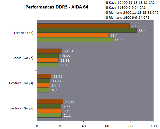
There's also a very substantial and rather odd increase in memory latency:
IMG0043802.png

http://www.hardware.fr/articles/913-5/cpu-protocole-ddr3-2400.html
Probably HSA related. The memory latency only went from horrendous to even more horrendous though all things considered (as intel does more than 3 times better...). Some compression benchmarks seem to lose out due to that on an IPC level compared to Richland.
On that front I'm not really convinced of that HSA implementation, yes coherency is a big step but now they've got even 3 memory links from the gpu. That's not what I'd call a fully unified northbridge...
 
Has anyone seen a review that compares the A10-7850k IGP with a HD7750 GDDR5/DDR3?

The results are just proof of the Pink Elephant in the Room: lack of memory bandwidth.

The only balanced solution is the A8 with 6 GCN CUs and a 45W TDP.
Above that, increasing the available power and number of CUs is worthless.

And why is there no comment from anandtech or anyone else about the presence of two 128-bit memory controllers in Kaveri?

I believe it has 2 x 64-bit, not 2 x 128-bit. It cannot be too much longer, 2015 perhaps until 3D stacked DRAM starts appearing on AMD APUs, the increase in bandwidth will be very welcome.

"And speaking of memory bandwidth, Kaveri has two 64-bit, fully independent memory channels. "We do stripe across them," Macri told us, "especially for the memory that's allocated for high-bandwidth needs like graphics."

Compared to discrete GPUs, 128 bits of memory bandwidth might seem – well, does seem – a bit paltry when compared with AMD's most powerful discrete GPU, which has a 512-bit bus. But as Macri points out in defense of the narrower path, Kaveri has just eight GPU cores to feed, whereas the hefty discrete-memory GPUs have more.

"We are a little light on memory bandwidth for graphics," he said, "but we're perfect, I think, on the compute side – or very close to being very well balanced on the compute side."

Source: http://www.theregister.co.uk/Print/2014/01/14/amd_unveils_kaveri_hsa_enabled_apu/
 
The poor CPU performance is what I figured was going to remain, but still disappointing to see. The GPU is obviously where they are doubling down but the terrible memory bottleneck makes it all for nothing I think. Anandtech has an old partially gimped Juniper stomping every modern iGPU. I imagine if Kaveri had double the bandwidth that wouldn't happen - at least when TDP isn't an issue.

They could sure make some tiny CPU dies if they dropped the huge IGP! Or make something like Intel Avoton....
 
The BKDG doc for Kaveri has been released recently... Apparently Kaveri was really supposed to be equipped with GDDR5 memory as a complement to the standard DDR3 one.

That would solve the mem b/w problems for 'hiend' SKUs at expense of a few watts more.

http://support.amd.com/TechDocs/49125_15h_Models_30h-3Fh_BKDG.pdf Search "GDDR5" string.

Regarding to the exotic memory configurations. The HBM/HMC solutions are surely pretty expensive ATM and it will need a few years/generations to get cheap enough for AMD's still-budget APUs.
 
If Kaveri was originally supposed to have 4 memory channels, with GDDR5 compatibility on at least some of those channels, it might explain why latency has increased: it's just due to higher complexity (which doesn't actually achieve anything since it's all disabled).

That's rather unfortunate.
 
"And speaking of memory bandwidth, Kaveri has two 64-bit, fully independent memory channels. "We do stripe across them," Macri told us, "especially for the memory that's allocated for high-bandwidth needs like graphics."
He is referring to the die shot (and the kernel patches disabling 2 of 4 logical memory channels) which seem to imply there's more there than just 2 64bit ddr3 controllers. If you look at anandtech's pictures, http://www.anandtech.com/show/7677/amd-kaveri-review-a8-7600-a10-7850k/4 the memory controllers grew a lot in size (on the bottom edge for kaveri, upper edge on llano/trinity).
Someone should ask amd why the memory controllers are so big :).
They could definitely need more bandwidth, gpu clock scaling is hilariously bad (e.g. here, http://www.computerbase.de/artikel/prozessoren/2014/amds-apu-kaveri-im-test/6/ - for 40% higher gpu clock you don't even get a 10% increase in performance...).
If you thought Kabini with its single 64bit memory channel was memory bandwidth limited, think again, Kaveri has just half the bandwidth/flop. On the upside though you get nearly the same performance with the much cheaper, 6 GCN cores 65W a8-7600 than with the 8 GCN cores a10-7850k (in games)...

If AMD wanted to enable quad-channel memory, wouldn't they need quad-channel compatible motherboards as well? Anyway if AMD wants to waste die space, then why not, they've got money to burn :p
 

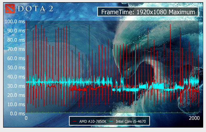
If you see graphs like this when the rendering time differs from frame to frame that much (that is, a very high frame time followed by a very low one) without using some AFR solution, this is usually a good indication that for some reason the measurement does not represent reality. That can happen pretty easily if you rely on dx to acquire this information.
 
The BKDG doc for Kaveri has been released recently... Apparently Kaveri was really supposed to be equipped with GDDR5 memory as a complement to the standard DDR3 one.

All I see about GDDR5 is a checklist in the memory section saying "GDDR5 isn't supported".
What they say is that only DCT0 and DCT3 can be used even though DCT1 and DCT2 are present.


I don't think the APU has GDDR5 support. First because I think a 2*64bit GDDR5 memory controller wouldn't look exactly like a 2*64bit DDR3 controller, which is what we see in the pictures.
Second, I also don't think they would mix the GDDR5 address space (DCT1+DCT2) between the DDR3 controllers (DCT0+DCT3).


Isn't this the manual for the A88X motherboards?
What are the chances for AMD to be releasing embedded solutions or a new family of motherboards (A89X?) with all four banks activated in the future?

It's just that the second pair of 64bit DDR3 controllers look like a terrible waste of transistors and area and worse of all: It looks like such a wasted opportunity to grab the iGPU market leadership..

The way things are, Kaveri is probably just going to be squashed by Broadwell..
Maybe the desktop motherboards/laptops with the 256bit memory are scheduled to release when Broadwell releases?


And just a question:
How would a 4-module SteamrollerB using 32nm SOI at current Vishera speeds and 8MB L3 cache?
Maybe quite closer to Intel's solutions?
 
Last edited by a moderator:
don't think the APU has GDDR5 support. First because I think a 2*64bit GDDR5 memory controller wouldn't look exactly like a 2*64bit DDR3 controller, which is what we see in the pictures.
We're seeing what looks like 4x64bit DDR3 there, not 2x64bit
 
The only way I can see Kaveri having any real market is if HSA/hUMA is extended to amd discrete cards and that there is some real performance/cost advantage in doing this.
I'm guessing only FM2+ motherboards with Kaveri CPU's will have the hardware capable of doing this.

Are cheap no memory discrete graphics cards feasible?
Would it have enough bandwidth if it plugged into more than one PCIe16 slot? i.e. a motherboard with two PCIe 16 slots next to each other.

Is it possible to reverse the problem and map the entire graphics card memory into the system address space and implement shared virtual memory for it.
Perhaps only pages marked as nonexecutable would be assigned to this memory.
Of course this would mean all CPU memory data accesses are going across the PCIe bus....

It would be cool if they could implement hUMA for graphics cards with dual gpus. i.e. share the card memory between the gpus on a dual gpu card. But again, would this give a performance advantage?
With existing dual gpu cards cards, when it uploads textures etc to both gpu's does it use broadcast pcie packets or does the driver upload to each in turn.

At a 1:16 fp64 rate and DP Gflops below that of a Intel CPU, Kaveri has no real value to me.
 
Are cheap no memory discrete graphics cards feasible?
Would it have enough bandwidth if it plugged into more than one PCIe16 slot? i.e. a motherboard with two PCIe 16 slots next to each other.
The idea that a DRAM-free board hanging off of PCIe can be cheap presupposes that a highly non-standard and standard-violating board with a dubious business case and non-standard GPU can be cheap.

If someone is so cost-conscious that even inexpensive DRAM is too much, you might be getting down to the most stripped-down and non-expandable motherboards you can find.
A graphics unit without access to local memory hasn't been practical since early in the last decade, and I doubt even the vaunted latency-hiding capabilities of a GPU can hide the impact of having no local framebuffer. The ROPs would probably be one of the first elements to falter, with the necessary batch sizes and local caching necessary becoming too large to be practical.
The following is more speculative, but pure PCIe accesses may also subject the GPU to more stringent ordering constraints than its aggressive memory pipeline can tolerate, negating the GPU's ability to utilize it well.

I would argue that AMD's APUs, or just dispensing with graphics hardware altogether have a higher upside.

Of course this would mean all CPU memory data accesses are going across the PCIe bus....
You'd probably save money and gain performance by just not bothering with the discrete board.

With existing dual gpu cards cards, when it uploads textures etc to both gpu's does it use broadcast pcie packets or does the driver upload to each in turn.
There are more complex transactions with modern PCIe, including things like broadcasting or endpoint to endpoint transfers. My limited understanding of it is that some kind of software process needs to perform it.
 
Back
Top