Vega users running regular radeon gaming driver:
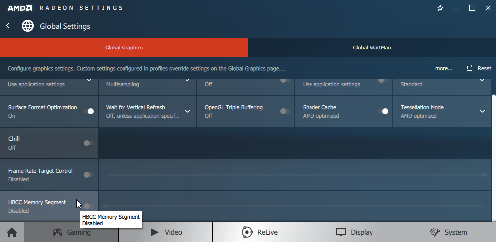
Do you have a HBCC slider in your radeon control panel --> global settings window? What about a compute optimization setting?
I have neither, and have never had either, not with any driver version, either signed WHQL or unsigned.
Do you have a HBCC slider in your radeon control panel --> global settings window? What about a compute optimization setting?
I have neither, and have never had either, not with any driver version, either signed WHQL or unsigned.
") Appreciate it!
Appreciate it!