AMD: Pirate Islands (R* 3** series) Speculation/Rumor Thread

The water-cooling was a consequence of using the HBM, not a reason for using HBM.
What's your problem with reading? I just wrote: "small size is a consequence of making a technology choice" (That choice being HBM)

With GDDR5 and water-cooler you will still need the immensely large PCB, it won't get smaller because of this.
Worst case, with a water cooler, the difference will be 26%. So much for 'immensely'. But that's an upper bound, since no GPU PCB other than FuryX has ever been designed to be used exclusively for water cooling.
 
GCN doesn't have any of these problems. Bad GCN multisampled performance in the tiled lighting shader are most likely explained by bad occupancy. If you don't use the all tricks in your book to force the AMD shader compiler to behave properly, you will end up with high VGPR usage in the complex tiled lighting shaders. Multisampled versions are much more prone to VGPR pressure, since the shader is more complex. I think we spent at least a month in optimizing the VGPR usage of our tiled lighting shader. But the end result is nice. We can push 16k visible lights at locked 60 fps (on a middle class GCN 1.1 GPU). It is silly how even simple things such as changing the order of two lines of shader code can cut the VGPR usage down by 2-3 (giving up to 10% extra performance for an shader that has poor occupancy).

Any idea, how GCN handles register spilling?
 
The bottom line is that HBM2 is a superior technical solution in every way. The deciding factor will be cost. If it's cheaper or at least pretty similar to implement a single stack HBM2 solution vs a 256bit GDDR5 solution then that's the way the mid and low ranges will go. If not, they'll stick with GDDR5. Since the high end parts will use HBM2 though and the mid range mobile parts will also benefit from it more, there may be an argument there that it would be cheaper from an R&D point of view to equip the entire range with that solution rather than going with two different memory solutions for the same core IP.
 
the PCB length is 7.7" vs 10.5", good for a PCB side reduction of just 26%

Only a quarter smaller which can actually make a difference day and night if the card would fit in the case or not.
You think that we are writing here just for the sake of argument but it was exactly the "good old" GDDR5 on 6870 (with its length of 290 mm) which FORCED me to buy a new case.
And it wasn't enough - I even needed to adjust the HDD cages..... :rolleyes:

then knock yourself out and go for a FuryX

Of course Fury X (or the Nano are the choice. I wonder how it is possible to ignore such fantastic innovative products.
 
ALU was a big bottleneck on last gen consoles, so it takes a while to change your code base and habits to be perfect fit for modern GPUs. GCN is not ALU bound in most shaders, but that doesn't mean that adding CUs shouldn't improve the performance (almost linearly), since additional CUs give a linear increase in total registers, L1 cache, LDS, etc (= many other potential bottlenecks in compute code).
Those things do need to be a bottleneck to see any difference though.

Compute shader optimizations in general doesn't "port" well across architectures. You get big performance differences simply by changing your thread group size (128 = 16x8, 256 = 16x16, 512 = 32x16, 1024 = 32x32 threads). Less than 256 threads per group doesn't suit GCN well. And 1024 threads per group (32x32 tile) is hopeless to get running at high enough occupancy (for any complex multisampled tiled lighting implementation).
I believe GCN won't accept more than a 256 work group size. I suspect larger is illusory.

Depending on the GPU resource bottlenecks, a different group size is optimal. If the same shader code is used on multiple generations of AMD and NVIDIA GPUs, the thread group size will likely not be perfectly optimal for each. Wrong thread group size is alone enough to severely hamper performance on some GPUs.
A few months back I wrote about apocryphal VGPR allocations in code I'm working on. Since then I've cleaved my kernel in two, with the rationale that I can't avoid storing data off-die for possible run times of 1+ seconds, since there's no way I can construct a pure on-die pipeline (which would also use multiple kernels).

Running two kernels compartmentalises VGPR and shared memory allocation. This enables me to re-code the two halves without fighting their joint VGPR+LDS allocation, which ultimately leads to more performance.

The two halves are strongly asymmetric in their use of VGPRs and LDS. The first half has a giant cache in LDS and moderate VGPR allocation, the second uses a small amount of LDS for 8-way work item sharing with a huge VGPR allocation including a large array in VGPRs. Luckily it has very little latency to hide (and it has huge arithmetic intensity), so 3 hardware threads isn't really a problem. The first kernel is LDS limited to 5 hardware threads. An improvement from 3 hardware threads for the uber kernel, which is where the performance gain came from as far as I can tell.

And now I have the freedom to re-work the first kernel now that it isn't bound 1:1 by the logic and in-register capacity constraints of the second kernel, e.g. I can run half the instances of kernel 1 for each instance of kernel 2, reaping more performance from the huge cache.

It helps that global memory access latency incurred by writing and reading data across the split is hidden, with only about 14GB/s usage. I now have the opportunity to re-code each half, which means I'll get substantially more performance than the original "uber kernel" (rather than the 3% gain I got doing the split).

Overall, it seems to me there's a lot of mileage in atomising kernels.
 
Only a quarter smaller which can actually make a difference day and night if the card would fit in the case or not.
You think that we are writing here just for the sake of argument but it was exactly the "good old" GDDR5 on 6870 (with its length of 290 mm) which FORCED me to buy a new case.
And it wasn't enough - I even needed to adjust the HDD cages..... :rolleyes:

These are personal needs based on what your case is, not a general perception or cost vs HBM, I think that is what Silent guy was getting at.


Of course Fury X (or the Nano are the choice. I wonder how it is possible to ignore such fantastic innovative products.

As innovative as they are, they are in competition with other products, if those innovations don't manage to fully help compete with a equal marketable product, they kinda die in the water :).

I still have more doubts about the Nano now than before after see what the Fury X has done.
 
Size: I believe that a GDDR5 GPU designed with water-cooling in mind right from the start can be made significantly smaller than the conventionally cooled GPUs of today. They just never bothered because the cooler needs to be big. We'll have to wait for the Fury to see whether that's really true or not. IMO, small size is a consequence of making a technology choice, but not a fundamental influencer of using that technology.

I don't think that's correct. The Fury Nano is air-cooled and even smaller than the Fury X. And NVIDIA has emphasized smaller size as one of the benefits of stacked memory, so it's not just AMD either.

Power benefits: the combination of HBM and a highest-end chip with an efficient core is going to be awesome. But if the next x04 chip from Nvidia in 14/16nm will be similar in performance to gm200, then it should consume significantly less power than gm200 while keeping GDDR5 and well below 200W, negating a strong need for the HBM power savings there.

It's a matter of nice to have vs necessity. More than extra BW, AMD needed HBM power savings as a band aid to stay borderline competitive. I expect them to fix their power efficiency issues with the process shrink. (After all, they must have been doing something worthwhile in their core logic in the last 3 years.) And Nvidia didn't need the power savings at all.

It would be complacent to forgo the power savings of HBM on the grounds that 14nm is enough. I think that's a recipe for losing market share, especially if the competition makes a different choice.
 
@sebbbi, why is it you think that AMD isn't fixing its shader compiler? I've seen here on B3D that developers have been dissing it since at least the radeon 5000 series IIRC. You dev guys should know perfectly well what is wrong with that compiler and I'm sure you've told AMD repeatedly why exactly it sucks. Why is it so hard to get it fixed? :p
The Microsoft HLSL intermediate byte code is still based on ancient vec4 format, and is designed for (DX9 era) GPU architectures that no longer exist. Intel, AMD, NVIDIA (and even mobile GPU manufacturers such as Imagination) are now all scalar based. The Microsoft HLSL -> byte code optimizer is doing much more harm than good. Vectorization adds often useless instructions, allocates useless registers, and sometimes transforms simple operations to something arcane (that used to be fast on old DX9 GPUs). Modern GPU vendor shader compilers need to first undo all these HLSL -> byte code optimizations and transform the vec4 byte code to scalar code.

A direct HLSL -> GPU microcode compiler is not a good idea on PC (OpenGL does this, and it causes lots of problems, since the GPU vendors need to write their own GLSL parsers, etc). Vulkan style (modern) intermediate language (SPIR-V) would be a perfect fit for DirectX as well. It would make the job of the GPU vendor shader compiler teams much easier. I am not sure how big compiler team AMD has, but competing against Intel and NVIDIA in compilers is not easy, since both of these companies have big compiler teams (on both CPU and GPU side). Architectures such as Denver, Itanium and Xeon Phi require highly sophisticated compilers to work. CUDA and supercomputers have been a big focus for NVIDIA (requiring robust shader compilers, supporting templates and other modern features). Intel's C++ compiler is one of the best (if not the best) C++ compiler for performance critical code. AMD doesn't even have its own C++ compiler.

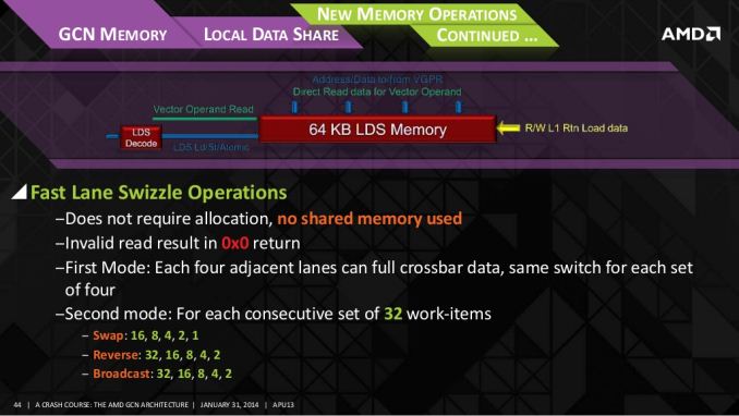
I would prefer that Microsoft adopted SPIR-V, since it would make cross platform shader authoring much easier, but I doubt that ever happens. HLSL has starting to show age compared to the modern shader languages, such as Metal (C++), CUDA (C++) and OpenCL 2.1 (C++). Different developers of course have different opinions about how the shader languages should evolve. One thing I would like to have in HLSL (or the next DirectX shading language) is cross lane operations. All the modern Intel, AMD and NVIDIA GPUs support cross lane operations, and with them you can write super efficient GPU primitives (such as prefix sums and reductions). If a new shading language surfaces, I just hope it has a good (platform independent) implementation for cross lane operations. Data type for "less frequent than per thread" data should also be present. It would allow the programmer to tell the compiler that some data doesn't need per thread storage (or computation). This would allow big savings in register space (and also allow scalar unit offloading on architectures supporting those).
 
I suppose you mean this ?
GCN 1.2 now has the ability for data to be shared between SIMD lanes in a limited fashion, beyond existing swizzling and other data organizations methods. This is one of those low-level tweaks I’m actually a bit surprised AMD even mentioned (though I’m glad they did) as it’s a little tweak that’s going to be very algorithm specific.

AMD_Swizzle_575px.jpg
 
The technology is interesting. But if performance and perf/$ are major concerns, it's not the obvious slam-dunk the AMD claimed it would be.

Yet aside from speculation you have absolutely no idea of the HBM's cost and how it compares to GDDR5, making your "perf/$" theory based on one big "if".
You can theorize all you want about how you think HBM is 5x or 10x more expensive per/GB than GDDR5 and you can still be very, very wrong.


For all factors that we can actually measure (performance, PCB footprint, power efficiency), HBM is a slam-dunk.
The problem about Fiji is that everything else isn't.

Fiji seems to be just a 2*Tonga with HBM and little else, and Tonga is a 10 month-old GPU.
I personally found the Fury X reviews boring as hell. There were no architectural enhancements over last year's GPUs at all.
I was hoping for an outrageous boost in geometry performance, an updated VCE with HEVC encoding at 4k60FPS for the ultimate streaming machine, HDMI 2.0, a substantial revision to GCN after 3.5 years, or whatever.
Instead, it's really just 2*Tonga, so everything that was new then is now old, and HBM was so hyped and detailed beforehand that we already knew almost everything about it.

All of this makes me look at the Fury X as a card that was simply delayed too much.
It should have never been released after the Titan X, much less the 980 Ti.
Had this card been available in time for Christmas 2014 and it'd have been a blast.
Plus, by now OEMs would've gained enough experience with the cards and would've released outrageously-clocked versions with unlocked voltages.
Instead, the 980 Ti cards are the ones gaining that upper hand, with little to no extra cost, making the choice between the competitors a rather easy one.
 
The Fury X, and "Pirate Islands" in general is just a stopgap after the new GPU architecture was delayed until next year. It appears a new architecture was originally being layed out for 20nm process, but with yields and etc. from manufacturers not allowing large/high heat dies that GPUs need it appears it was delayed until next year and 14nm. AMD of course still needed something, so they just doubled Tonga with a few slight changes and came up with the Fury X.

It's not really a bad chip, for where most people would be buying it (to run games at 4k) it does about as well as a 980ti, and since it has a similar price it might sell well enough as a stopgap. The Nano is also a neat use of cold/low frequency binned chips. They might be able to charge $600 for it as it'll be a limited run (depending entirely on yields). Being smaller, faster, and having less power draw than a 980(non ti) will certainly hit the perfect niche for some people.


I don't think it was a stop gap, it was a back up plan in case 20nm flopped which it did. In 10 months there would have been no way for AMD to make Fiji, it was already been designed and in simulations a year or maybe even two years ago. As TottenTranz stated, its not a bad chip but timing when released was bad, this might have been do to the mass production of HBM.

Also doing limited runs isn't a way to get a company that is heavily in debt out of trouble, that would be short term thinking. After the Fury X launch does it seem like Nano, an air cooled piece have a performance per watt advantage vs. a 980? Doesn't look like it. So either the power consumption is going to more then the gtx 980 or its performance will be lower. Its not like the architecture is going to be different......
 
Overall, it seems to me there's a lot of mileage in atomising kernels.
Yes. We have also noticed that simpler kernels are almost always a win, if the split doesn't cause a big extra BW cost. With DX12 you can precisely control which compute shaders are running simultaneously by placing (or not placing) resource barriers between them in the command queue. You don't even need async compute for this. So you have a pretty straightforward way to instruct the GPU run two shaders simultaneously, even if those are accessing the same resources (this obviously only works as long as you know what you are doing). In DX11, the API was highly conservative, and didn't allow this to happen (wasting GPU performance).

I also hope that we get kernel side enqueue (spawn lambdas as kernels) to DirectX soon. This allows much finer grained shader execution. With the current GPU execution model with static (worst case) register allocation, small sub kernels lauched by the GPU are a good way to reduce the register pressure. This way you only pay for the uncommon branch when you actually hit it, and you can also split the shader efficiently to smaller parts.

We obviously need a better (on-chip) way to communicate (pass data) between these shaders. Now we need to trust the caches. As both NVIDIA and AMD have raised their caches to 2 MB this might actually not be that big problem (Intel has had big GPU caches as long as I remember).
I suppose you mean this ?

AMD_Swizzle_575px.jpg
Yes, those are the GCN 1.0 lane swizzles. NVIDIA has similar (see CUDA documentation) and Intel has released some OpenCL 2.0 examples and benchmark results of their cross lane swizzle gains. Andrew most likely could give you some extra full details (or a link to a ISA document, if one is publicly available for Broadwell GPU).
 
HBM is a slam-dunk.
I don't think I would go that far. Actually, I'd say HBM1 is kind of meh. The performance is good but not great, and the density limitations were a bit unfortunate (for the high-end). It seems like it would have worked ideally this gen for mid-tier cards (and notebooks) except for the cost.

However, I do think HBM2 will be a slam-dunk. It is just straight up better in every way and not by a small amount. Given the progress of integrated graphics, I'm not even sure there is really a place for the "low-end" anymore. HBM2 vs GDDR5 for mid-tier cards might appear to be a toss up at first, but I would think the power efficiency advantage in mobile applications would tip the scale in favor of HBM2.
 
I don't think it was a stop gap, it was a back up plan in case 20nm flopped which it did. In 10 months there would have been no way for AMD to make Fiji, it was already been designed and in simulations a year or maybe even two years ago. As TottenTranz stated, its not a bad chip but timing when released was bad, this might have been do to the mass production of HBM.

Also doing limited runs isn't a way to get a company that is heavily in debt out of trouble, that would be short term thinking. After the Fury X launch does it seem like Nano, an air cooled piece have a performance per watt advantage vs. a 980? Doesn't look like it. So either the power consumption is going to more then the gtx 980 or its performance will be lower. Its not like the architecture is going to be different......

We already know the Nano is going to have a performance advantage over a 980, if only slight. Taking the quote of 2x performance per watt over a 290x and a 175 watt tdp at face value we get a 16% increase in performance (rounding down) over a 290x, faster than a 980, and at 175 watts, while slightly higher than the 980's 165 watts (I was remembering it as 190 watts somehow, oops) but still better performance per watt. Combined with its relatively tiny size it's valuable to the right crowd.

And the Nano is almost certainly a binned Fury X, as it will have reportedly a fully enabled chip. For those that don't know, not all silicon comes out of the manufacturing process the same, and these differing chips will be "binned" and sold differently depending on how they came out. One outcome is that a chip won't be able to hit the target frequency at the voltage it's supposed to. This means the chip won't perform to the target spec, but comes with the advantage of less static leakage than the nominally "hot" chips that can. This is almost certainly the Nano, with it's probably 800mghz or so frequency but much less heat output, thus needing only a small air cooler, and why there will only be limited quantities of such, because they are in effect unwanted defects, but still valuable.
 
Even with binning, how much can they save? Lets take a look at this

http://www.techpowerup.com/reviews/AMD/R9_Fury_X/32.html

Depending on resolution, Nano, if I take your numbers which you got from AMD's press conference, to get around 16% faster then a 290x and at 175 watts, it would need a power savings of 26 to 59% give or take a few.


I think that is quite excessive for just binning chips. And we aren't even getting to the point of air cooling yet. If they are able to do that form just binning, what the hell is going on with the Fury X :runaway:

Yeah they will clock it down some, but to get the performance and power usage to the gtx 980 levels that 26-59% is still a pretty big obstacle.
 
Last edited:
Even with binning, how much can they save? Lets take a look at this

http://www.techpowerup.com/reviews/AMD/R9_Fury_X/32.html

Depending on resolution, Nano, if I take your numbers which you got from AMD's press conference, to get around 16% faster then a 290x and at 175 watts, it would need a power savings of 26 to 59% give or take a few.


I think that is quite excessive for just binning chips. And we aren't even getting to the point of air cooling yet. If they are able to do that form just binning, what the hell is going on with the Fury X :runaway:

Yeah they will clock it down some, but to get the performance and power usage to the gtx 980 levels that 26-59% is still a pretty big obstacle.

TDP scales exponentially with frequency, not linearly. Depending on frequency, assuming your normal target frequency is somewhere just beyond the "takeoff" portion of the exponential curve, you can save a lot of power by clocking down say, 30% or so and save the 40% or so power you'd want. The GPU makers of course don't do this most of the time as it's usually better to hit that 5%-30% better performance even if you're taking 6-40% more power to do it.
 
I don't think that's correct. The Fury Nano is air-cooled and even smaller than the Fury X. And NVIDIA has emphasized smaller size as one of the benefits of stacked memory, so it's not just AMD either.
- The Fury Nano is a very cute GPU, and when priced right, it will find plenty of takers. But it seems to be the lemonade that you make out of a lemon rather than one that you plan to make right from the start. I have my doubts about how sustainable it is commercially in the long term. It's going to be pretty bad in terms of production cost/perf compared to what it replaces/competes with.
- I'm not saying a GDDR5 GPU can be made as small as an HBM GPU when using the same cooling, just that a water cooled GDDR5 GPU can probably made smaller than the current crop of air cooled GDDR5 GPUs. Of course HBM has the benefits of smaller size. But will the Fury be as small as the FuryX? I highly doubt it. So the area savings of using HBM, without performance being crippled like the Nano, will be somewhere between 0 and 26%.

It would be complacent to forgo the power savings of HBM on the grounds that 14nm is enough. I think that's a recipe for losing market share, especially if the competition makes a different choice.
Look at all the reviews of FuryX. Everybody is quite enthusiastic about AMD finally be somewhat competitive against Nvidia. And about power being much better. And about the size of the card. And then... it all deflates when they say how it should have been a bit cheaper compared to the 980Ti.
If one uses HBM and the other doesn't and perf is the same, the other will have a significant pricing leverage.

BTW: I don't see this as an AMD vs Nvidia thing. IMO for the next generation, both will continue to use GDDR5 for everything but the highest SKUs.
 
Yet aside from speculation you have absolutely no idea of the HBM's cost and how it compares to GDDR5, making your "perf/$" theory based on one big "if".
You can theorize all you want about how you think HBM is 5x or 10x more expensive per/GB than GDDR5 and you can still be very, very wrong.
Nobody said HBM would be 5x or 10x more expensive per GB than GDDR5. I wrote 'low integer factor'. Think 2x, 3x.

For all factors that we can actually measure (performance, PCB footprint, power efficiency), HBM is a slam-dunk. The problem about Fiji is that everything else isn't.
And an very interesting follow-up question would be: how much better would a gm200 with HBM be? Because that's ultimately the key: for a particular performance segment, how much do you need the awesome bandwidth of HBM. There is no question that next gen top dogs will make very good use of HBM. The gm200 and the Fiji successors will absolutely need it. But the discussion is about their smaller brethren, where cost is more of factor because you're targeting market segments that are inherently more cost sensitive. Where you can expect gm200/Fiji performance on a smaller technology node. Where you will have excess bandwidth with no enough core shader power to make use of it. Where you will have less of a crippling power wall.
 
Back
Top