Doomtrooper
Veteran
Xbox uses Hypertransport on the IGP, I never stated it uses Hyperthreading.
") j/k
j/kmisae said:I'd feel muh better if you called me a moron or something DT.
Those smileys are scaring me.

Xbox uses Hypertransport on the IGP, I never stated it uses Hyperthreading.
Doomtrooper said:Xbox uses Hypertransport on the IGP, I never stated it uses Hyperthreading.
Panajev2001a said:g_day, I will point one flaw of what you said... the GeForce FX is not 120+ MTransistors dedicated to ONLY execution units... I am sure the occlusion detection HW, the cross-bar based memory controller, the caches take quite a bit of transistor logic as well....
these are logic circuits that control something, they make decisions - they are execution units not data.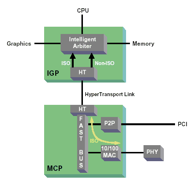
Doomtrooper said:Yes Grall and the IGP is the 'effective Northbridge' of the X-box....a CPU doesn't need to support Hypertransport....
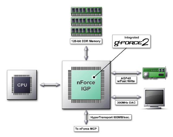
If you actually go back to the previous page and study what you wrote, you'll see this: "To me the above is more important than slight performance increases running a couple of tasks...the Hyperstransport traces coming off that lowly PIII 733 is one of the good reasons why X-box graphics blow away alot of PC titles." Hint: P3 lacks RAM controller also, so why would there be DDR chips positioned around the *P3*? Conclusion: pic does not show P3.Grall said:I'd say the reason XB titles looks better is because they actually target DX8-level graphics, which ye average PC title does not. But hey, that's just me of course.
*G*
And I still state that the Hypertransport is one of the reasons why the X-box can produce great graphics with basically a PIII 733 PC .Code or data - execution logic or cache - they are your choices - by mentioning occlusion detection HW, the cross-bar based memory controller you are arguing my case these are logic circuits that control something, they make decisions - they are execution units not data.
Game, set, match.
How can you compare a 3GHz CPu having 12GFLPOS max with a 500MHz chip having more like 400 GFLOPs counting the vertex and pixel shaders combined?
So clock per clok cycle is 400/12*3/0.5 = 200 more powerful, and its doing 128 bit precision maths - not 32 bit precision -
The Xbox doesn't have to rely on the CPU for graphical computations. Pretty much all the work is done on the NV2A and the CPU is left for physics, AI, etc.And I still state that the Hypertransport is one of the reasons why the X-box can produce great graphics with basically a PIII 733 PC .
Panajev2001a said:First, in order to reach that number you're counting everything down everywhere in the pipeline from texture fecth to set-uo to rasterization to texture filtering, T&L, etc... every single op everywhere...
My comparison is pretty much on the T&L side as I can see myself that purely software rasterization would bring the Pentium 4 down quite a bit ( still if you did do rasterization with integer based math [maybe FIXED point arithmetic] you should go quite fast... nowhere as fast as a modern GPU in that regard as the Pentium 4 was NOT designed for it )... but T&L should be handled pretty well by the Pentium 4 including dynamic tesselation and deferred T&L if you wanted to program it... the Pentium 4 could sort the incoming vertex stream and try to T&L only the visible polygons... if HOS were used you could try to tessellate oly the visible patches by sorting at the control points level and then tessellating... sorting the incoming stream of vertices or of HOS control points is a good serial task that requires speed and lots of bandwidth... which the Pentium 4 has...
The Pentium 4 can do the same 128 bits math as the VS if we go by your definition... SSE works with 128 bits vectors as well
All of that hardware and power is there for a reason. It might not all get used all the time, but in order to change that 400GFlop figure to a 12 GFlop fligure you are assuming that the hardware is only running at about 3% utilisation - anyone who creates 3D hardware that runs at that sort of efficiency is insane, and going out of business real soon.
And that's assuming that the processor runs at 100% utilisation. Unlikely.
Yes - you can run geometry pretty fast on a modern CPU - current processors are capable of rates in the same ballpark (within 1 order fo magnitude, certainly) to current VPUs, if you just look at calculation throughput. However efficient data movement is a big problem, and you can easily find yourself limited by data transfer rates.
) yeld 6.4 GB/s of total bandwidth... ( 1 MB.... yummy )...Yup , but it's strictly vertical SIMD and never horizontal. By this I mean that it always does x*x, y*y, z*z, w*w (or swizzled versions of this). It doesn't natively support the most useful instructions (dot products x*x+y*y+z*z+w*w), although this can be worked around.
In the general case it's just difficult to come close to the execution efficiency of dedicated hardware vertex shaders, which is why such a huge clock rate advantage is required.
The CPU logic hardware is generally only 5% busy because it follows a linear standard Neuman based design; fetch instruction, decode, fetch memory addresses execute store etc. Its a powerful general computing device - not an incredibley parallel, specialised chip. A GPU doing 3D processing always has thirty things happening at once in comparision, its a far more parallel peice of hardware.
How am I arguing your case ? Then we should have all the branch prediction logic, the reaname registers and the ReOrder Buffer, the prefetching unit, the cache tag logic, the Control Unit and all the logic that goes with it ( which includes micor-memory for the VISCier instructuions... the trace cache receives only a "pointer" to Control Memory for those to avoid filling the trace cache with u-ops for these very uncommon instructions... ) etc... those are logic circuits which control something and that make decisions...
