Install the app
How to install the app on iOS
Follow along with the video below to see how to install our site as a web app on your home screen.
Note: This feature may not be available in some browsers.
Artificially as in: limited by SW? Or is the hardware just not there? (In which case it isn't really artificial...)I was saving this for my review, but since I'm a bit behind schedule...
Under CUDA, FP16 performance (in FLOPs) on GTX 1080 is artificially limited to 1/64th the FP32 rate. Technically this is actually 1/128th the instruction rate, but due to vec2 packing you get twice the FLOPs out of a single instruction.
My belief is software, just like FP64 perf on GTX 780 and the like. A 1/128 instruction rate is not something that can reasonably be done in hardware, since FP16 uses the FP32 CUDA cores and those all need to be identical.Artificially as in: limited by SW? Or is the hardware just not there? (In which case it isn't really artificial...)
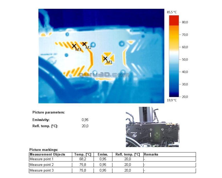
I went the MSI 970 over the G1 because of its size. The G1 is much larger and wouldn't fit in my case. The MSI provides excellent cooling for its size.And you can see the results in the respective reviews from guru3d
MSI: http://www.guru3d.com/articles_pages/msi_geforce_gtx_980_ti_gaming_oc_review,10.html

GB G1: http://www.guru3d.com/articles_pages/gigabyte_geforce_gtx_980_ti_g1_gaming_soc_review,10.html

I'm sure it's not a big deal in general but if i'm spending almost $1k on a GPU i'd want the best thing around, i went with a G1 last time around just because of the cooling solution and the overall experience has been great. That's all irrelevant if you are going with water of course.
Edit:
The 390x you mentioned has active cooling for the vrm and passive for the vram
https://www.techpowerup.com/reviews/MSI/R9_390X_Gaming/images/cooler2.jpg
https://www.techpowerup.com/reviews/MSI/R9_390X_Gaming/images/cooler3.jpg
So it might be better than the one used for the 1080.
Ext3h
Regular
Uh, isn't there vectorized ops on the GP100? The code sample from which these were generated, did the compiler have the option to vectorize it?The exact same SASS instructions are generated for sm_60 (GP100), sm_61 (GP104) and sm_62 (GP???):
Code:sm_60: HFMA2.FTZ R10, R0, R5, R6; /* 0x5d0003200057000a */ sm_61: HFMA2.FTZ R10, R0, R5, R6; /* 0x5d0003200057000a */ sm_62: HFMA2.FTZ R10, R0, R5, R6; /* 0x5d0003200057000a */
The open question is throughput.
We now know it's not 256 ops/clock like in the Tegra X1 (sm_53) and assumed to be in the GP100 (sm_60).
128 fp16 FMAs per clock would be excellent but at this point I'm betting that it's closer to 16 since anything higher should've been trumpeted!
pixelio
Newcomer
The code sample from which these were generated, did the compiler have the option to vectorize it?
The code was generated from explicit PTX but CUDA intrinsics would have the same result.
pixelio
Newcomer
... since FP16 uses the FP32 CUDA cores and those all need to be identical.
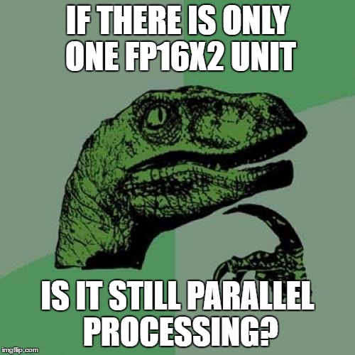
It seems more likely they're dedicated units?
My original guess of 16 ops/clock imagined that 8 fp16x2 units (16 fma16/clock) would've shipped paired with 8 FP64 units (4 fma64/clock) lifted from the GP100.
We'll all know soon once CUDA devs start digging.
Or NVIDIA could just tell us.
I consider that highly unlikely. Not only does that break architectural symmetry (GP100 doesn't have dedicated units), but that would prevent NVIDIA from selling these as Tesla parts in the future.It seems more likely they're dedicated units?
Thx for sharing that, I did not want to forestall.I was saving this for my review, but since I'm a bit behind schedule...
Under CUDA, FP16 performance (in FLOPs) on GTX 1080 is artificially limited to 1/64th the FP32 rate. Technically this is actually 1/128th the instruction rate, but due to vec2 packing you get twice the FLOPs out of a single instruction.
FP16 support on GTX 1080 is solely for binary compatibility reasons, and suffice it to say, NVIDIA made sure that's all it is good for.
Conveniently, it is also 1/2 the DP-FP or FP64 rate. Going through there would allow for binary compatibility as well as allow Nvidia to carbon copy their older ALUs at least wrt "native" FP16 support.Under CUDA, FP16 performance (in FLOPs) on GTX 1080 is artificially limited to 1/64th the FP32 rate. Technically this is actually 1/128th the instruction rate, but due to vec2 packing you get twice the FLOPs out of a single instruction.
FP16 support on GTX 1080 is solely for binary compatibility reasons, and suffice it to say, NVIDIA made sure that's all it is good for.
Last edited:
A1xLLcqAgt0qc2RyMz0y
Veteran
I was saving this for my review, but since I'm a bit behind schedule...
Under CUDA, FP16 performance (in FLOPs) on GTX 1080 is artificially limited to 1/64th the FP32 rate. Technically this is actually 1/128th the instruction rate, but due to vec2 packing you get twice the FLOPs out of a single instruction.
FP16 support on GTX 1080 is solely for binary compatibility reasons, and suffice it to say, NVIDIA made sure that's all it is good for.
Speaking of FP16. Will you be getting a DGX-1 for review?
http://www.nvidia.com/object/deep-learning-system.html
Not currently scheduled. We haven't traditionally reviewed Tesla products, and with Tesla P100, NVIDIA is already selling it faster than they can make it.Speaking of FP16. Will you be getting a DGX-1 for review?
http://www.nvidia.com/object/deep-learning-system.html
Alessio1989
Regular
I am sorry, but this architecture is becoming every day more hilarious.. Fortunately they improved the rasterizer a lil...
Because FP16 doesn't matter for hardly anyone but the deep learning crowd. It's perfect for their Tesla deep learning accelerators.What kind of madness is deliberately gimping FP16 to a tiny fraction of FP32? Why even do that?
Hilarious or not, it's a great way to create a very profitable business. What's the alternative? Giving away everything and yelling"We're open!" ?I am sorry, but this architecture is becoming every day more hilarious.
It wasn't artificially gimped in earlier architectures, just the same rate as FP32. THAT's a decision i can hardly follow.Because FP16 doesn't matter for hardly anyone but the deep learning crowd. It's perfect for their Tesla deep learning accelerators.
Similar threads
- Locked
- Replies
- 10
- Views
- 1K
- Replies
- 166
- Views
- 10K
- Replies
- 788
- Views
- 141K
- Replies
- 12
- Views
- 2K

