Nvidia Pascal Announcement

Isn't that what I said when I said quote

or am I messing something up?
Yes, you are. You don't want to hit that maximum. Ever. If you do, you loose the ability to utilize all cores, due to lack of concurrent warps.
And you can't just scale the register file size up (without other drawbacks), so you just don't. Instead you scale the SM cluster in total down, and add more of them. Increasing latency and decreasing throughput of each individual warp, but improving overall throughput, especially in worst case.
 
Kind of interesting that P100 has been targeted for deep learning when its real killer feature is a staggering 5TFLOPS of FP64 operations.
 
Last edited:
I'm guessing the Pascal Titan will be the GP102. I think it'll take a looong time for GP100 to appear as Geforce, if ever... GP104 coming first with X80 and X70 models and GP102 later as Titan and X80 Ti or something like that.
 
Nope, they are dedicated. And I guess Nvidia will iterate the consumer (desktop/mobile) SKUs into their own compute capability version (6.1 and 6.2) with some additional ISA changes.
Any other sources for this than the rather illustratively purposed block diagram? :) Contrary to a 1:3 ratio, 1:2:4 ratio lends itself quite naturally to multi-purposed units, IMHO.
 
They might do. But GDDR5X will do that bandwidth. Why aim so low?
The preliminary numbers for GDDR5X make it better in terms of power per unit of bandwidth relative to GDDR5, but still inferior to HBM and by extension even more so than HBM2.
Nvidia makes a point of citing HBM2's native ECC, and the standard also has room for a few other items like a thermal failsafe and row hammer mitigation, which access-happy HPC might appreciate.

Then there's the footprint of GDDR5X PHY which is unclear, while GP100 also needs to devote perimeter to 64 20 Gbs lanes for NVlink (I recall something like that footprint for AMD's rumored HPC APU and/or the GMI links).
 
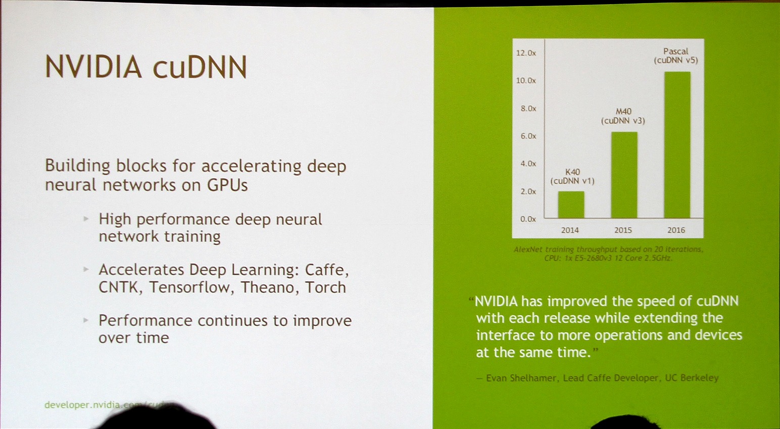
Pascal Deep Learning performance claimed by Nvidia:
IMG0050217_1.jpg


Source: http://www.hardware.fr/news/14574/gtc-deep-learning-70-pascal.html

Sorry if someone else has picked up on this but only got time now to post:
I was trying to find correlation figures pertaining to Alexnet/imagenet peformance to put this chart into a better context.
The closest I could find relates to the Titan X that managed 450 images/sec (from official NVIDIA slides), it could be deemed the Titan X was better specc'd in this context than the Tesla K40 so some allowances would need to be made for the figures to be a bit lower.

So is expanding that would suggest Maxwell M40 manages around 2,700 images/sec, and the new Pascal-cuDNNV5 replacement manages around 4,500 images/sec.
Give or take due to the Titan X/K40 differences, and very rough ballpark figures.
Cheers
 
Kind of interesting that P100 has been targeted for deep learning when its real killer feature is a staggering 5TFLOPS of FP64 operations.
Agreed, it's interesting. I think they might be more worried about competition with Intel in the HPC market than maximising efficiency for deep learning, where they already have a huge competitive advantage (especially in software, but also increasing on the hardware side with FP16).

For GeForce, I hope we'll see a fully enabled 60SM GP100 Titan this year (SHUT UP AND TAKE MY MONEY!!!) but it sounds possible we might see GP102 and/or GP104 before that. It's intriguing that NVIDIA has a chip with a '2' as the last digit, They haven't had one since G92 (where G90 was missing). This could mean a smaller difference in performance than usual (e.g. 3072 SMs without FP64 or NVLINK?) where GP100 is *only* released as a Titan outside of the professional market or not at all.
 
I wonder how those 5 TFLOPS of DP will turn out in practice. After all, compared to GM200, P100 has eight times as many ALUs to feed from it's same-sized register files. Compared to GK110 it's only half though.
 
... where GP100 is *only* released as a Titan outside of the professional market or not at all.
Not going to bet on it, but my guess is going to be a Titan P with full 64 SMs, and a GTX 1080 Ti with 56.

Also, sometimes later next year, a 32GB variant.
 
I frankly don't see them releasing a full SM version any time soon, if ever.

The beauty of having tons of identical cores is that disabling a few is almost invisible. See GTX 980 Ti vs Titan X.

The cool thing about redundancy and random faults is that the benefits of redundancy are largely uncorrelated with the size of the redundant block: if you have 30 blocks and you disable 1 of them, your benefit won't be much better than having 60 and disabling 1.

However, your benefits go up significantly with the number of redundant blocks. 1 redundant block out of 30 is much less effective than 2 out of 60, even though it makes no difference in terms of redundant area. My theory is that Nvidia split the SMs in half for this reason. With a smaller granularity, they can exploit this benefit.
 
rumored GP102 makes sens. GP100 is too much HPC oriented to be viable as a consumer product. It also means that GP100 is the first GPU exclusively dedicated to HPC. At such performance leap with DGX1 on trendy deep learning market, they must have a long queue of customers wanting for this new toy.
hmmm maybe time to buy some NVDA shares $$$$$$$

GK210 would like a word with you...
 
However, your benefits go up significantly with the number of redundant blocks. 1 redundant block out of 30 is much less effective than 2 out of 60, even though it makes no difference in terms of redundant area. My theory is that Nvidia split the SMs in half for this reason. With a smaller granularity, they can exploit this benefit.
Yea, it's kind of a trend since Kepler -- each generation comes out with more compact multiprocessor design. By the time for Volta Nvidia will bring it full circle back to Fermi. :p
 
I don't know why, but my spider sense tells me there is something quite not right with nVIDIA presentation today. Deja vu from Fermi times?
- No actual hardware presented,
- Jen did not seem his usual very enthusiastic self, the hesitation about arriving time, concluding with "soon",
- 300W GPU on a new fabrication process right off the bat (when HBM2 is supposed to be more energy efficient than GDDR5)
- No GPU roadmap (possibly the first time one is not shown at a GTC?).
- Since nvLink was developed in cooperation with IBM, isn't it weird that IBM was not there at all?
- Yes, there were lots of references of companies going to, or intending to use Pascal, but we've seen how design wins worked for Tegra in the past.
- Talking about Tegra, where was it? Shoehorned into Drive PX2 with barely an honor mention?
- I did not get what was the point of spending so much time presenting VR demos on stage that couldn't obviously be experienced by the audience there, plus a cringe worthy cameo by Steve Wozniak.. Yey, we spend infinite amounts of time recreating Mars... because we can.
By the end of the presentation I was freaking bored, which is not usual for nVIDIA's.

EDIT - Plus one disturbing fact: there was not a SINGLE demo where they said it was running on Pascal! Even on Fermi presentation, with all the clusterfuck going on behind closed doors, Jen demoed things supposedly running on Fermi. Now they say Pascal is going to volume production and do not care to even show a single demo, but just pretty charts?
 
While it's interesting to see any number of things confirmed, the most surprising is the just apparent scaling of the whole thing. 600mm already (cough, no release date and the only mention is Tesla aka super high end and very high price). But... that's all they got out of 600mm? They can't scale more on this process, at all. And just a 66% jump on the highest end?

Is HBM2 really that big? I mean, geeze. It's not like the transistors to performance even scaled linearly, hell it dropped. We have a 66% (approximate) performance improvement from an 87.5% increase in transistors. With HBM 2 and finfet Pascal manages to be worse, transistor per transistor, than Maxwell. A 12% drop in efficiency is not what you want out of a node jump and "architecture jump" at all.

In its way it's similarly impressive in the same way Nvidia has done in the recent past, aka make a huge chip. But the limited ram (16gb) for an exclusively high end card (AMD puts out 32gb cards already for their highest end) and the rather disappointing performance for a new node already being maxed out for size is... well hopefully Volta works out well for Nvidia next year. Which is not to say 66% wouldn't be impressive in its own right, but the Tesla line costs a hell of a lot so it doesn't seem like, price for performance wise, this is going to be all that attractive for a while.
 
You're talking about spec sheet performance. Let's see how it turns out in the real world.
 
Mr. Pony, when you forget the double sized register files, and 1:2 FP64 ratio, you shouldn't be surprised that your efficiency numbers are a little bit off compared to a chip that doesn't have it.

As for comparisons with AMD: they don't play in the market, so it doesn't matter.
 
While it's interesting to see any number of things confirmed, the most surprising is the just apparent scaling of the whole thing. 600mm already (cough, no release date and the only mention is Tesla aka super high end and very high price). But... that's all they got out of 600mm? They can't scale more on this process, at all. And just a 66% jump on the highest end?

Is HBM2 really that big? I mean, geeze. It's not like the transistors to performance even scaled linearly, hell it dropped. We have a 66% (approximate) performance improvement from an 87.5% increase in transistors. With HBM 2 and finfet Pascal manages to be worse, transistor per transistor, than Maxwell. A 12% drop in efficiency is not what you want out of a node jump and "architecture jump" at all.

In its way it's similarly impressive in the same way Nvidia has done in the recent past, aka make a huge chip. But the limited ram (16gb) for an exclusively high end card (AMD puts out 32gb cards already for their highest end) and the rather disappointing performance for a new node already being maxed out for size is... well hopefully Volta works out well for Nvidia next year. Which is not to say 66% wouldn't be impressive in its own right, but the Tesla line costs a hell of a lot so it doesn't seem like, price for performance wise, this is going to be all that attractive for a while.
Well for now you would need to compare the Tesla to the Fiji Pro model, and its HBM is limited to 1 or 2x4GB, on the plus side for AMD is at least you can buy it soon.
I must admit I am surprised any 600mm with high clocks is already achievable even if yields are appalling, the rumours made it sound like we would not see anything like this soon from either TSMC or Samsung-GF and were reinforced that only low power/small GPU models have been seen to date or talked about.
I wonder how close AMD with GF are themselves to something comparable; meaning can achieve benchmarks (the big Pascal looking at the presentation did seem to be used as they mention data based on 20 iterations for the Alexnet) and not necessarily actually to be released soon.

I guess NVIDIA will be cagey about release schedule and especially for consumer models as they do not want to tank current sales.
Cheers
 
Back
Top