I don't have anything serious (no discrete article anyway that I can have ready) by now, so I think I'm going to post some details and just talk about it on the forums until I've got something formal ready. HD 5870 needs finishing first really anyway.
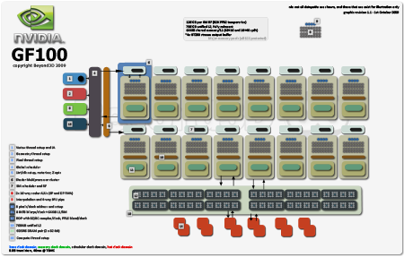
The big highlights (some is guesswork, NV won't talk about graphics transistors or clocks today, so beware I might be wrong in places there):
3.0B transistors @ TSMC, 40nm
2 x 16-way FMA SM, IEEE754-2008, 16 SMs
Each SM has four SFUs
384-bit GDDR5
~650/1700/4200MHz (base/hot/mem)
8 pixels clock address and filter per SM
48 ROPs, 8Z/C clock
64KiB L1/smem per SM (48/16 or 16/48 per clock config, not user programmable as far as I know, at least not yet)
Unified 768 KiB L2 (not partitioned now, so a write to L2 from any SM is visible to all others immediately)
Unified memory space (hardware TLB, 1TiB address, 40-bit if my brain's working)
Each SM dual-issues per clock on two half warps, for two clocks. Instructions can be mixed, so FP+INT, or FP+FP, or SFU+FP, etc. If DP instructions are running, nothing else runs. Although I don't think that's quite right, need to run some CUDA on a chip to test.
1.5K threads per SM in flight (1K in GT200), 32K FP32 registers per SM (up from 16K in GT200).
DP is half rate as mentioned, and it's a FMA too. All memories the chip talks to, from registers up, are ECC protected (potentially, nobody ships ECC GDDR5, and I think the chip will address 'PC' DDR3 for that in the end). Not sure what scheme or penalty.
New generation of PTX, CUDA 3.0. C++ in CUDA because of the unified address space.
Some new predication support, although it's really not clear how the hardware makes it happen. Seems you can predicate any instruction.
New atomic performance. Seems like it'll coalesce atomic ops in a warp and won't hit DRAM if the update fails, instead using L2 (GT200 replayed the transaction at DRAM hundreds of clocks later). The whitepaper explanation is wrong.
Seems RF per SM has enough ports (256) and support from the operand fetch hardware to sustain full FMA rate across the chip.
It can run multiple CUDA kernels now at the same time. Limit is 16 per chip (one per SM), but I think that'll be capped at 8.
I think the tesselator is a software pipe with very little hardware support, too.
Anyway, that's from memory, more later when I'm free.

If you want more, dkanter's ready with his (and it's excellent) here.
The big highlights (some is guesswork, NV won't talk about graphics transistors or clocks today, so beware I might be wrong in places there):
3.0B transistors @ TSMC, 40nm
2 x 16-way FMA SM, IEEE754-2008, 16 SMs
Each SM has four SFUs
384-bit GDDR5
~650/1700/4200MHz (base/hot/mem)
8 pixels clock address and filter per SM
48 ROPs, 8Z/C clock
64KiB L1/smem per SM (48/16 or 16/48 per clock config, not user programmable as far as I know, at least not yet)
Unified 768 KiB L2 (not partitioned now, so a write to L2 from any SM is visible to all others immediately)
Unified memory space (hardware TLB, 1TiB address, 40-bit if my brain's working)
Each SM dual-issues per clock on two half warps, for two clocks. Instructions can be mixed, so FP+INT, or FP+FP, or SFU+FP, etc. If DP instructions are running, nothing else runs. Although I don't think that's quite right, need to run some CUDA on a chip to test.
1.5K threads per SM in flight (1K in GT200), 32K FP32 registers per SM (up from 16K in GT200).
DP is half rate as mentioned, and it's a FMA too. All memories the chip talks to, from registers up, are ECC protected (potentially, nobody ships ECC GDDR5, and I think the chip will address 'PC' DDR3 for that in the end). Not sure what scheme or penalty.
New generation of PTX, CUDA 3.0. C++ in CUDA because of the unified address space.
Some new predication support, although it's really not clear how the hardware makes it happen. Seems you can predicate any instruction.
New atomic performance. Seems like it'll coalesce atomic ops in a warp and won't hit DRAM if the update fails, instead using L2 (GT200 replayed the transaction at DRAM hundreds of clocks later). The whitepaper explanation is wrong.
Seems RF per SM has enough ports (256) and support from the operand fetch hardware to sustain full FMA rate across the chip.
It can run multiple CUDA kernels now at the same time. Limit is 16 per chip (one per SM), but I think that'll be capped at 8.
I think the tesselator is a software pipe with very little hardware support, too.
Anyway, that's from memory, more later when I'm free.

If you want more, dkanter's ready with his (and it's excellent) here.
Last edited by a moderator:


