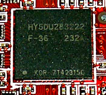
Help with BGA Memory modules

Dave Baumann

Gamerscore Wh...
Moderator
Legend
This Digit Life review looks at both the Radeon 9500 and Radeon 9700 from Gigabyte. And it looks at the BGA memory modules.

As we can see the main difference between the 9500 and 9700 for the memory bus is that they have just removed half the chips to make the 128-bit memory bus. My understanding is that the BGA modules account for 32bits of bus width per module, so for the 9700 PRO each module accounts for part of the 256bit bus. This means, to my understanding, that each of the modules is 128MB to account for the correct amount of RAM on a 256bit bus.

Now, the 9500 has half of its bus removed and is only 64MB, so my understanding would be that each of the modules are are only 64MB to make the 64MB on a 128bit bus. However, the HYNIX part number (HY5DU283222 F-36) for the memory used in this case list the modules as being '128M', which to me indicates 128MB of memory.

I'm obviously missing something here, so if anyone can clear up my misconceptions it would be appreciated! :)
 
If this is the case then my question moves on to more fundamental memory bus structures.

How is the data distributed to ensure maximum utilisation of the bus for the the capacity of the RAM available?
 
DaveBaumann said:
If this is the case then my question moves on to more fundamental memory bus structures.

How is the data distributed to ensure maximum utilisation of the bus for the the capacity of the RAM available?

Most likely, data are striped across the modules at a rather fine granularity. Given that R300 uses a crossbar with 64-bits width per channel and a burst length of 2, each memory access is at least 128 bits long. If you then try to access multiple consecutive 128-bit blocks, you will presumably end up hitting each memory channel in turn (this is guesswork; the block size may be larger, like 256 bits, but the principle is the same). This layout gives good bus utilization for both long sequential accesses and lots of random accesses, and any combination thereof.
 
DaveBaumann said:
Now, the 9500 has half of its bus removed and is only 64MB, so my understanding would be that each of the modules are are only 64MB to make the 64MB on a 128bit bus. However, the HYNIX part number (HY5DU283222 F-36) for the memory used in this case list the modules as being '128M', which to me indicates 128MB of memory.

Uh... wait. If Radeon 9700 cards have eight 16 Megabyte (128 Megabit) / 32-bit RAM chips, that means they have 8 * 16 = 128MB on an 8 * 32 = 256-bit bus.

If instead Radeon 9500 cards have FOUR 16 MB / 32-bit RAMs, that means 4 * 16 = 64 on a 4 * 32 = 128-bit bus.

I don't see the big problem here. o_O They're still 16MB chips... if you have half as many chips, using half-sized chips would result in 32MB! :LOL:
 
http://www.ixbt.com/video2/sapphire-r9500-128.shtml
there is a R9500 128MB review in ixbit, maybe these picture can explain

the most important thing is Radeon9500 128MB and Radeon9500 64MB are use same RAM(HY5DU283222 F-36, 32X4M= 16MB per chip )
sapphire-r9500-128-mem.jpg


Radeon 9500 128MB

sapphire-r9500-128-scan-front-small.jpg

sapphire-r9500-128-scan-back-small.jpg


Radeon 64MB
r9500-scan-front-small.jpg

r9500-scan-back-small.jpg


[/img]
 
That 128MB 9500 looks like it was still using the full 256-bit bus width...

I think that was the point of the article. ;)

That they seem to be actually implying that the shipping 128 MB Radeon 9500 cards will run with a 256 bit bus. Dunno how realistic that is...my suspicion is that they just have some engineering prototype that doesn't reflect the actual end product. Or perhaps they confused a Radeon 9700 non-pro with the Radeon 9500 non pro. (On a related note, I thought all 9500 non-pros were supposed to only have 64 MB?)

Doesn't make any sense to me that a 128 MB Radeon 9500 non-pro would use different memory than a 128 MB Radeon 9500 Pro: 128 bit bus.

EDIT (addition):

It does strike me now that we have yet to see ANY p/review of a 128 MB Radeon 9500 part (this xbit peek excluded.). IIRC, ATI is suppossed to have a redesigned PCB for the 128 MB Radeon 9500 PRO...presumably one of the reasons is to be able to effectively handle memory chips with 1/2 the density of the ones used on the 128 MB 9700s, and 64 MB 9500s.
 
No, what they have reviewed there is basically a 9700 (non-pro), not a 9500. The point being is that manufacturers have not got true 9500 boards through yet, so they are not using the memory bus correctly.
 
Mr.huang said:
http://www.ixbt.com/video2/sapphire-r9500-128.shtml
there is a R9500 128MB review in ixbit, maybe these picture can explain

the most important thing is Radeon9500 128MB and Radeon9500 64MB are use same RAM(HY5DU283222 F-36, 32X4M= 16MB per chip )

It's ok to use the same dram chips between the two boards. What will then happen is that for the 128MB board you will have 2 of the chips sharing a data line. This is what the gf4 does to support 128MB on a 128-bit bus, and it is also what the nv30 sample boards were doing (judging from the pictures). I think they call it "TwinBank" or some other sort of marketing non-sense.
 
9700 Pro = $400
9700 = $300
9500 Pro = $200
9500 = $150

I dont see a reason for the 9700 (non pro).
 
misae said:
9700 Pro = $400
9700 = $300
9500 Pro = $200
9500 = $150

I dont see a reason for the 9700 (non pro).

9700 Pro = $400 = 256bit bus/8pipe/(325/310)
9700 = $300 = 256bit bus/8pipe/(275/275?)
9500 Pro = $200 = 128bit bus/8pipe
9500 = $150 = 128bit bus/4pipe


Seems to make sense to me the lineup and pricing...
 
misae said:
9700 Pro = $400
9700 = $300
9500 Pro = $200
9500 = $150

I dont see a reason for the 9700 (non pro).

It's the idea of having "almost" the fastest card (which might actually be obtained with overclocking) but paying $100 less for it (9700 compared to 9700 Pro.)

Same principle exactly with the Ti4400 and the Ti4600 by nVidia & OEMs at their introductions.
 
BobbleHead said:
It's ok to use the same dram chips between the two boards. What will then happen is that for the 128MB board you will have 2 of the chips sharing a data line. This is what the gf4 does to support 128MB on a 128-bit bus, and it is also what the nv30 sample boards were doing (judging from the pictures). I think they call it "TwinBank" or some other sort of marketing non-sense.

Ahh, that's what I figured. I recall the 128MB 8500 boards also having 8 4Mx32 chips on them. It also explains why the redesign has all eight chips next to each other.

Thanks for the explanation. Does this mean the 9700 chips are 8Mx32?
 
WaltC said:
misae said:
9700 Pro = $400
9700 = $300
9500 Pro = $200
9500 = $150

I dont see a reason for the 9700 (non pro).

It's the idea of having "almost" the fastest card (which might actually be obtained with overclocking) but paying $100 less for it (9700 compared to 9700 Pro.)

Same principle exactly with the Ti4400 and the Ti4600 by nVidia & OEMs at their introductions.

I agree with you in part but the 9500 Pro seems to be doing pretty well in terms of performance compared to the 9700 Pro.
 
The R300 was designed to be able to handle 64b, 128b or 256b memory operation. In each of the cases, the design is capable of distributing data evenly accross all bits the bus. There's never a "prefered" BGA; the mems are not setup in a simple sequential organization.

As far as the 9500Pro vs. 9700 vs. 9700 pro, the 9500pro is an excellent product, but it will not compare to a 9700 or a 9700pro at higher resolutions or in more demanding applications. In fact, it can be 1/2 the speed of a 9700/9700pro in some cases, due to having only 1/2 the BW. The 9700 is just a slower clock version of the 9700pro, so it should scale well compare to the 9700pro (i.e. 20% slower, or whatever the clock ratios is).

The 9500pro obviously has a great price performance, and does very well compared to all products, especially at lower resolutions. However, you will discover that it does not overclock much (if at all), compared to the 9700pro.

The initial reviews might of been done on full 9700 boards, with 2 channels disabled. That's exactly the same as having 128b bus, like the 9500x series. The currently shipping 9500pro does not have a 256b bus; not sure, but I believe it's 4 BGAs, so 64MB/4 = 16MBytes per BGA, and each is 32b wide.
 
DaveBaumann said:
Mintmaster said:
Thanks for the explanation. Does this mean the 9700 chips are 8Mx32?

Samsung 9700 PRO memory=1M x 32Bit x 4 Bank

Hynix 9500 PRO memory=4x32

Both parts are 4Mx32. The naming for memory devices is to list the number of bits per data I/O and the data I/O bus width. So a 4Mx32 part is 4 Mb/pin (megabit, not megabyte), and is 32-bits wide. The total density of one device would then be 128 Mb (megabit). Slap 8 of them onto a card and you've got 128 MB (megabyte).

The specific organization is another issue. There are 2 bank, 4 bank, and (now) 8 bank devices. So you could take a 128Mb, 4Mx32 device and it might be 2M x 32Bit x 2 Bank, 1M x 32Bit x 4 Bank, or 0.5M x 32Bit x 8 Bank.

The sample pictures of the nv30 also use 4Mx32 devices (1M x 32Bit x 4 Bank), and there are 8 of them, arranged much like the memory on a 9500Pro board. Both have 128MB of memory.

I wonder now about the rumors of a 256MB nv30 board. No 8Mx32 DDR2 devices are around at the moment, and with only 4Mx32 to use, you'd have to put 4 of them on a single data line. It'll be pretty difficult (or impossible) to get that to work at any reasonable speed. That points to nv30 boards being limited to 128MB for a little while.
 
Back
Top