Haswell vs Kaveri

I guess I still don't see it. The radically-altered Pentium they showed, when running at "NTV levels", was ridiculously low performance. I guess you might argue that a metric ton of these processors, all simultaneously running in a Beowulf cluster (LOL) might be able to pump out a few TF, but the supporting power for connecting that many chips would be insane

I guess conceptual problem I'm having is this: NTV provides far lower-powered X86 processing. I agree that it indeed significantly increases flops/watt per chip, but only when operated at very, VERY low power (and thus, in absolute terms, low performance) modes. Hell, the Atom does better than any of the Core architecture for flops/watt, but I don't (yet) see anyone making supercomputers out of them. If we wanted a race to ultimate flops/watt, we'll be doing custom SoC stuff.

THoughts?

True. And you are pointing at a couple of issues yourself - power draw of memory and communication will remain unchanged per FLOP. Even in the pure bragging rights parts of the HPC market, this kind of solution makes even less sense than putting a bunch of GPUs in a cabinet (*cough*).

But on the other hand thinking machines actually produced a couple of 2^16 processor (single-bit) computers back in the day, so it's not as if systems have to make much sense from a production point of view to be produced in a research environment.
 
But on the other hand thinking machines actually produced a couple of 2^16 processor (single-bit) computers back in the day, so it's not as if systems have to make much sense from a production point of view to be produced in a research environment.
They did and for the time that "CPU" was actually one of the fastest in the world for solving general computational problems as well. Fancy stuff :)
 
True. And you are pointing at a couple of issues yourself - power draw of memory and communication will remain unchanged per FLOP. Even in the pure bragging rights parts of the HPC market, this kind of solution makes even less sense than putting a bunch of GPUs in a cabinet (*cough*).

But on the other hand thinking machines actually produced a couple of 2^16 processor (single-bit) computers back in the day, so it's not as if systems have to make much sense from a production point of view to be produced in a research environment.

Oh yeah, absolutely agreed on the research front. Nothing I've brought up was intended to be an argument against the research side of things; this is all very valid and important work that will have obvious implications for future production devices.

The difficulty I was having was the connection between NTV and Exascale. One is meant for epic low power under very low usage patterns; one is meant for an absolute (specific) computational throughput within a given (2KWhr?) power constraint. I agree that you could bundle 1mSt (Metric Shit Ton :D ) of NTV-capable processors running at NTV spec to generate that kind of absolute computational throughput, but you'd be WAY outside the power budget when considering the whole system.
 
I'm not sure that can be done easily within the same units.

The description of NTV design indicates that the transistors, architecture, and circuits are physically different in order to compensate for challenges unique to operating at that low a voltage.

Transistors doped to work at near threshold aren't going to behave the same when jacked up to turbo levels, and the circuits tuned to handle problems at NVT may not be needed or could pose an impediment to reaching normal voltage clocks.

That doesn't rule out having NVT on the same chip, and possibly in specific parts of a single core, but I don't know if areas of silicon that are tuned to operate at NVT (mW at MHz) will scale to turbo (tens of W at GHz) too well.
Possibly, the chip can "switch gears" and switch to NTV areas, with latency costs.

NTV could be part of Intel's answer to big.LITTLE
 
It could be used to produce a low-power state where an active core can downshift from turbo, then down to normal, and then instead of a sleep state or a context shift to a little core, it can start sending instructions to an NTV domain.

It wouldn't be as power-efficient in the long-idle state, but it would be much more graceful and transparent to software. Low-usage scenarios where the idle periods are not long enough to justify the power cost of transitioning from power gated states or can't tolerate the latency of switching cores would benefit.


NTV may significantly bolster the diversification of silicon area. Specialized silicon or coprocessors can already produce several times the throughput in a fraction of the power.
A design optimized for NTV could make that fraction of the power even smaller.
This might explain why one of the concepts shown was a graphics SIMD unit.

The primary cost at the moment seems to be a loss of high-speed circuit performance, possible complications in the manufacturing process, and additional circuitry needed to combat variability and maintain reliability at those voltages.
Specialized hardware can be designed to not need high clocks, tends to be more regular, and the common tendency to have higher area density can offset the cost of NTV.
 
It could be used to produce a low-power state where an active core can downshift from turbo, then down to normal, and then instead of a sleep state or a context shift to a little core, it can start sending instructions to an NTV domain.

It wouldn't be as power-efficient in the long-idle state, but it would be much more graceful and transparent to software. Low-usage scenarios where the idle periods are not long enough to justify the power cost of transitioning from power gated states or can't tolerate the latency of switching cores would benefit.

Yup, this is exactly where I see it. Having a processor that's just "barely running" is conceptually far less latency than one that needs to recover from S3, while perhaps using only a small fraction of power above that S3 state. Enough to capture an interrupt, speed up enough to process it (or perhaps, decide not to) and then slow back down. An operating system that can do interrupt aggregation could significantly benefit from this.

Imagine being able to have the box go into the "SuperS1" state with the display still powered. Your keystroke could generate an interrupt that could be handled within the nearest few hundred cycles (ie, quite lazily), the screen updated, and the box may never have to be more busy than that. The processor draw for an 'office use' laptop could go to less than a watt for a box that could be perceived as perfectly responsive.
 
It could be used to produce a low-power state where an active core can downshift from turbo, then down to normal, and then instead of a sleep state or a context shift to a little core, it can start sending instructions to an NTV domain..

Will that fit what Intel said as "EIST C7/C10 State" supported by Haswell?
 
Yup, this is exactly where I see it. Having a processor that's just "barely running" is conceptually far less latency than one that needs to recover from S3, while perhaps using only a small fraction of power above that S3 state. Enough to capture an interrupt, speed up enough to process it (or perhaps, decide not to) and then slow back down. An operating system that can do interrupt aggregation could significantly benefit from this.

Imagine being able to have the box go into the "SuperS1" state with the display still powered. Your keystroke could generate an interrupt that could be handled within the nearest few hundred cycles (ie, quite lazily), the screen updated, and the box may never have to be more busy than that. The processor draw for an 'office use' laptop could go to less than a watt for a box that could be perceived as perfectly responsive.
So....It will be a new state between so-called EIST C1 and C3?
 
Who knows, I'm mostly just making crap up :D Maybe you're more correct, maybe it isn't a "sleep" state but rather some even deeper version of EIST. I dunno.
 
Will that fit what Intel said as "EIST C7/C10 State" supported by Haswell?

C1 and above have the core clock off, which would not be consistent with a NTV mode.
That may mean having NTV hanging around in the main pipeline isn't practical. It would require a lower range to the C0 state that may be more complex than it is worth.


One interesting thing about NTV is that it is much easier to stack chips that burn mW than those that burn 10-100.
 
Peformance of 28nm Bulk should be lower than the 32nm SOI right?

If thats the case Kaveri's CPU performance may not actually improve, and could actually take a step back :???:
 
Peformance of 28nm Bulk should be lower than the 32nm SOI right?

It depends. The advantage PDSOI (what GF uses) gives goes down with every shrink, and it might not give that much anymore. On the other hand, the 28nm shrink buys shorter distances, and possibly improved materials. It's essentially impossible to call without intimate knowledge of both processes.
 
Fuad claims that Kaveri will support DDR3 2133 memory (which is more of an obvious logical step rather than a crystall ball prediction), and Nordichardware claims there'll be a "Cape Verde Pro" inside it: 512 GCN sp, 32 TMUs, 16 ROPs, at 900MHz.


With a total of of 35GB/s of memory bandwidth and being the first "true" UMA architecture from AMD, how close can a Kaveri come to a discrete HD7750?

The whole APU will have about half as much bandwidth as the original discrete graphics card.
 
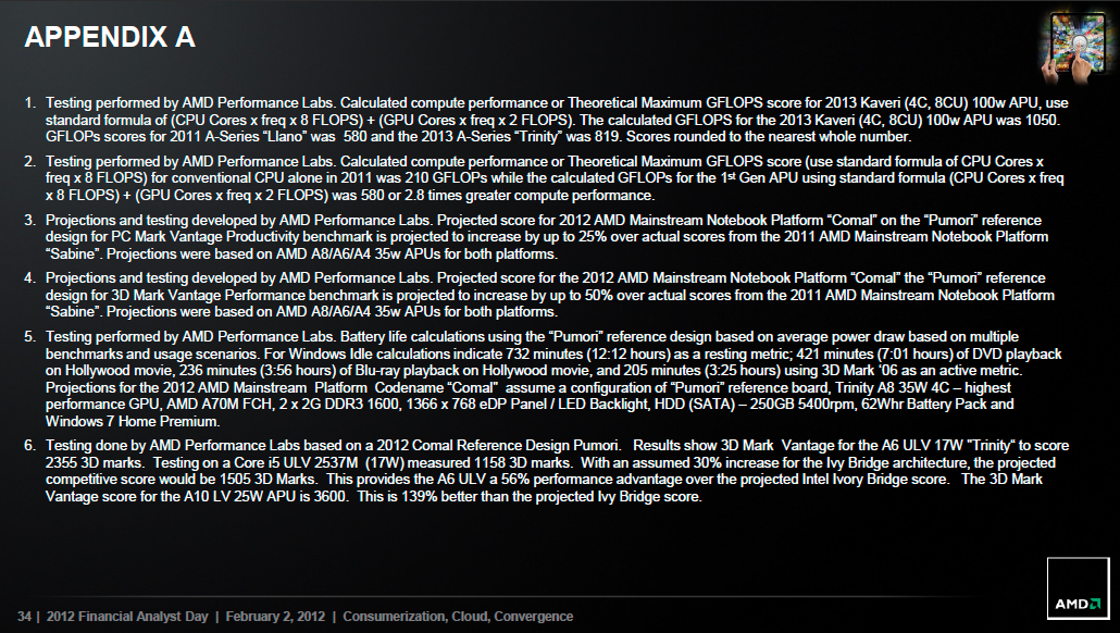
AMD gave that (8 CUs with GCN architecture) away by themselves in a footnote of some slide (financial analyst day).
kaveri_slidetualp.png


the full presentation
 
Last edited by a moderator:
With a total of of 35GB/s of memory bandwidth and being the first "true" UMA architecture from AMD, how close can a Kaveri come to a discrete HD7750?

The whole APU will have about half as much bandwidth as the original discrete graphics card.
I think if they get the whole integration (with llc sharing etc.) right it could probably get close even if it only has half the bandwidth. Otherwise (with llano-like integration) it would stay well below hd5750, might probably only match a 6670 or thereabouts. I've got no idea though how integration looks like on kaveri.
 
With a total of of 35GB/s of memory bandwidth and being the first "true" UMA architecture from AMD, how close can a Kaveri come to a discrete HD7750?

Not very. The chip will be really bandwidth-starved. The curve of performance/resolution will be very steep...

Also, I am skeptical of the 16 rops. To put it frankly, it won't be able to keep them fed -- might as well drop to 8.
 
That slide says to count 8 flops/core/clock for the CPU. No 256b AVX 2 years later still?

There's no need. In every fp benchmark I've done on BD that resemble real workloads, the performance is limited by the memory subsystem (more the caches than the memory controller), not the execution units.

Until they do some really heavy work on the caches, the dual 128-bit units will be just fine.
 
Back
Top