Haswell vs Kaveri

AnarchX

Veteran
Haswell
GMA Gen 7.5
40 EUs @ GT3
stacked DRAM
~5x SNB Gfx

VS

Kaveri
512SPs GCN @ >900MHz

APPENDIX A said:
Testing performed by AMD Performance Labs. Calculated compute performance or Theoretical Maximum GFLOPS score for 2013 Kaveri (4C, 8CU) 100w APU, use standard formula of (CPU Cores x freq x 8 FLOPS) + (GPU Cores x freq x 2 FLOPS). The calculated GFLOPS for the 2013 Kaveri (4C, 8CU) 100w APU was 1050. GFLOPs scores for 2011 A-Series “Llano” was 580 and the 2013 A-Series “Trinity” was 819. Scores rounded to the nearest whole number.
http://phx.corporate-ir.net/External.File?item=UGFyZW50SUQ9MTI1MTM5fENoaWxkSUQ9LTF8VHlwZT0z&t=1
 
We have had 12 EUs in Sandy Bridge, we gonna have 16 EUs in Ivy Bridge and Haswell will jump to 40 EUs? Maybe 40 smaller Larrabee cores? I'm wondering why this big jump from 16 to 40.
 
Haswell
GMA Gen 7.5
40 EUs @ GT3
stacked DRAM
~5x SNB Gfx
The semiaccurate report is bonkers, even if the hard numbers are true (which I don't know, 40 EUs looks like a big jump, then again if they have 3 versions it's quite possible).
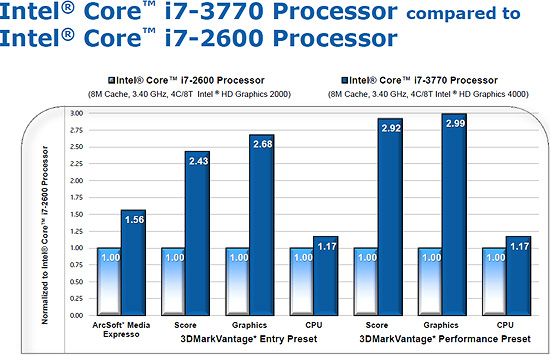
First, intel itself doesn't claim IVB is twice as fast, and it doesn't quite look that way (it is nearly twice as fast in 3dmark Vantage Performance score, but below that on Vantage Entry, I don't think this will result in twice as fast on average for typical apps).
But claiming just because of 2.5 times the EUs it has to be at least 2.5 times as fast even if there were no other improvements is very wrong. Just ask AMD how they achieve perfect scaling when only scaling the number of shader units... Doesn't mean it potentially couldn't be that fast (and I don't doubt they will shrink the gap to AMD or could even catch it in case AMD doesn't manage to get some better integration for more effective bandwidth) but certainly not just because of the increased EU count.
 
We have had 12 EUs in Sandy Bridge, we gonna have 16 EUs in Ivy Bridge and Haswell will jump to 40 EUs? Maybe 40 smaller Larrabee cores? I'm wondering why this big jump from 16 to 40.
An EU is much smaller than a core, a transition to LRB cores would have resulted in a drop in the number of units.

If the 40 number is accurate, there are a few trends that can lead to this.
Haswell is bigger than Ivy Bridge, and it is possible that the share of the die allocated to the GPU is higher.
There's a fair amount of non EU area in the GPU that doesn't scale as quickly with EU count, so the overall area in the GPU for execution resources could be higher.
Intel wants to appeal to a very broad client base for the various GT grades, and it's easier to have too much GT and fuse parts off from a too-big GPU than to custom fit it.

On top of that, it seems probable that Intel increased the GPU's share of resources because it can. In terms of power and circuit performance, the GPU may be able to operate in a voltage/frequency range that means that it matches a more optimal spot in the 22nm process. This means TDP and general consumption can be less sensitive to a big chunk of graphics hardware.

AMD's Llano had a sensitivity to how hard the CPU cores were pushed, and a less strong correlation to GPU grade. The reasons for that may not apply to Haswell, though it should be noted there are mobile variants with low TDPs and lower CPU grades, but with competitive graphics grades.
 
We have had 12 EUs in Sandy Bridge, we gonna have 16 EUs in Ivy Bridge and Haswell will jump to 40 EUs? Maybe 40 smaller Larrabee cores? I'm wondering why this big jump from 16 to 40.
The leaked photo of Haswell shows that the core has some quite disproportional dimentions. If the general layout is kept similar to SNB, this may give a hint to the die area dedicated for the IGP part:

http://4.bp.blogspot.com/-wbCxRI00O...013-Haswell-Processor-Reportedly-Pictured.png
 
Probably he got a new Roadmap. Vantage Entry is more CPU dependent.

The leaked photo of Haswell shows that the core has some quite disproportional dimentions. If the general layout is kept similar to SNB, this may give a hint to the die area dedicated for the IGP part:

http://4.bp.blogspot.com/-wbCxRI00O...013-Haswell-Processor-Reportedly-Pictured.png


GT1/GT2/GT3, 2 core or 4 core, we don't know the version.
An EU is much smaller than a core, a transition to LRB cores would have resulted in a drop in the number of units.

Unlikely then. I wouldn't be surprised if Charlie turns out wrong with the 40 EUs.
 
What Charlie does not take into account is the bandwidth problem. Even if you double-and-a-half the number of EUs, you'll need to keep them fed somehow. Otherwise it's just idle silicone which Intels seems to go to great lengths lately to avoid.

Given what Intel told a while ago in their IVB presentations about the graphics, I can imagine there being more variants than before. They claim to have an almost completely decoupled front end and except for IVB graphics, there's only one occasion outside pizza hut where I've recently stumbled upon the word "slice": iLRB.
 
I highly doubt that given the performance of the cpus and igps in question...


Compare Entry results between Llano and Sandy Bridge, they are much closer than it should. Vantage Performance lowers CPU dependency. Do you have an entry Vantage GPU score from i7-2600?
 
Compare Entry results between Llano and Sandy Bridge, they are much closer than it should. Vantage Performance lowers CPU dependency. Do you have an entry Vantage GPU score from i7-2600?
Well i was using the intel number of 2.68 times faster IVB compared to HD2000, which is only the graphics portion, not including cpu score. That won't really be dependent on cpu (even for the total score it was 2.43 times faster, so the cpu dependency is there but still not that big).
If SB and Llano are indeed closer there in the graphics portion of the entry score (couldn't find any quick numbers) than they "should" be, it's much more likely because it is because this benchmark part just suits intel igp relatively better (like more dependent on memory bandwidth, and/or can make good use of that cache) rather than any cpu dependency.
 
Well i was using the intel number of 2.68 times faster IVB compared to HD2000, which is only the graphics portion, not including cpu score. That won't really be dependent on cpu (even for the total score it was 2.43 times faster, so the cpu dependency is there but still not that big).

It is important. i7-2600 features a HD2000 with 1350 Mhz, all other CPUs have a lower clocked GPU.


If SB and Llano are indeed closer there in the graphics portion of the entry score (couldn't find any quick numbers) than they "should" be, it's much more likely because it is because this benchmark part just suits intel igp relatively better

Here: http://www.legitreviews.com/article/1644/11/

Entry Scores are meaningless for the much faster iGPU.

edit: I just looked into the overall score, Entry GPU score seems to be fine.
 
It is important. i7-2600 features a HD2000 with 1350 Mhz, all other CPUs have a lower clocked GPU.

2600 HD2000 scores ~ 1000 points in Vantage Performance, 6k in Entry.

igp-3dmv-p.jpg


http://www.pcper.com/reviews/Proces...y-Bridge-Processor-Review/Intel-HD-Graphics-3


The numbers intel used don't really match that well though. If you follow their only given benchmark then the 3770K could score between 2300 and 2900 Vantage points depending on whether the overall or gpu score is used,.

intel_ivy_bridge_performance_2.jpg


Either way, it's a lot slower than Trinity 25W scoring 3600 in Vantage.
 
Problem is: Intel quotes 2600 with HD2000. Smoke screen or typo? If the latter: Typo wrt to CPU or IGP, i.e. a 2600/HD3000 or 2500/HD2000.
 
Problem is: Intel quotes 2600 with HD2000. Smoke screen or typo? If the latter: Typo wrt to CPU or IGP, i.e. a 2600/HD3000 or 2500/HD2000.


No problem, we know it. There is no i7-2600 with HD3000, they all have a HD2000, no typo in the slide. We are talking about HD2000 in i7-2600.
 
In very old roadmaps Gesher (old codename for SNB) was projected to have Fast DRAM (512MiB@64GB/s). It seems it was shifted to the next architecture.

But I think this approach is more targeted on the SoC version of Haswell, to provide a high package bandwidth a low power and only one external module of ULV DDR3 could be enough to feed the CPU+GPU.
 
No problem, we know it. There is no i7-2600 with HD3000, they all have a HD2000, no typo in the slide. We are talking about HD2000 in i7-2600.

Ah, you're right. I was thinking, the free multiplier was the only thing they change from 2600 to 2600k, but they also upgraded the graphics. Damn. :)
 
I think we're probably missing the obvious: 40 EUs doesn't mean they increased other units by the same amount - I'd certainly agree they'd likely be very bandwidth limited if they did. However ALUs are the least bandwidth-hungry part of modern GPUs (doesn't mean they can't increase it somewhat, but nowhere near as much) so if you've got die area to spare it's nearly always a good way to increase peak performance for ALU-heavy workloads.
 
Back
Top