EDRAM in GPUS

loekf2 said:
Hmm... companion chip ? Why is it then called eDRAM in the first place ?

b3d16.gif


As you can see, Custom Memory 40 has some extra stuff going on.

You can read the patent:

http://patft.uspto.gov/netacgi/nph-Parser?patentnumber=6873323

Jawed
 
If they're separate chips, could they be on some sort of MCM package then, or would that not give any performance benefits over a more usual two-black-things-on-the-motherboard approach?
 
loekf2 said:
Hmm... companion chip ? Why is it then called eDRAM in the first place ?

someone said it's called enchanned DRAM. So, another excelent example of misuse of terms.

and what comes to claimed 256GBit/s transfer rate to eDRAM, they would need a 5120 bits wide bus to achieve it with 500MHz clock rate. If it's DDR bus then it's half of that, but still way too much to be put in between two cores. (although it goes inside single package, but still just too much.)
 
Nappe1 said:
loekf2 said:
Hmm... companion chip ? Why is it then called eDRAM in the first place ?

someone said it's called enchanned DRAM. So, another excelent example of misuse of terms.

and what comes to claimed 256GBit/s transfer rate to eDRAM, they would need a 5120 bits wide bus to achieve it with 500MHz clock rate. If it's DDR bus then it's half of that, but still way too much to be put in between two cores. (although it goes inside single package, but still just too much.)

it's probbaly called eDRAM as it includes addtional logic to do z-compare and blending
 
The leak for XB360 says 4gigapixels per second and the presumption is that's 8 bytes per pixel, i.e. 32GB/s.

Who knows, eh :?:

Jawed
 
Is it called eDRAM because it's eDRAM that is "embedded" on a helper chip. But I still think it's a little disingenuous labeling, whether intentional or not, because everyone's first thought is that the eDRAM is on-chip on the R500 just like VRAM on PS2 and that it would have an amazingly large bus-size.

Moreover, using "effective" bandwidth numbers in the specs further lead to confusion, since the only way one could get such high numbers (if you didn't read the fine print "effective") would be from some amazing large 2048bit bus to eDRAM inside the core.
 
DemoCoder said:
Moreover, using "effective" bandwidth numbers in the specs further lead to confusion, since the only way one could get such high numbers (if you didn't read the fine print "effective") would be from some amazing large 2048bit bus to eDRAM inside the core.
What about real bandwidth between R500 and memory chip then? Got any numbers?
 
The way MS is calculating is simple: two quads with 32bit color read and write (blending) and Z-stencil test and write with 4xMSAA at 500MHz.
2 * 4 * (4 + 4 [read] + 4 + 4 [write]) * 4 * 500M = 256GB/s

This however is a bit misleading on several levels. First, do they mean bandwidth between the two chips, or bandwidth from ROPs to memory like in "traditional" architectures? Presumably the former, but that isn't comparable to external memory bandwidth figures.

Assuming they mean bandwidth between the two chips...
color and Z data is never read across that connection, because only the ROPs need this data. For the same reason, stencil data is neither read nor written, because a fragment has no associated "stencil data", that only exists in the framebuffer.
Furthermore, color data is identical for all samples in a pixel and Z data can be encoded as gradient per quad. The only thing that's needed additionally for AA is a coverage mask.

So disabling blending, Z-test, Z-writes, stencil test, stencil writes, or AA practically "saves" no bandwidth - the connection can be considered a multitude of dedicated channels.

Overall, what is required per quad are 4* 32bit color, compressed Z (3 * 24bit at most) and 4* 4bit of coverage mask, meaning less or equal to 216bit per quad. And since there may be two quads per clock with color, that's at most 432bit required for the connection between the two chips, which equals 27GB/s.

Assuming they mean bandwidth from ROPs to the memory array...
then 64bit (32bit color + 31bit Z/stencil + 1bit flag) need to be read and written per pixel. That means 512bit for reads and writes each are required, equalling 32GB/s for reads and 32GB/s for writes.

(That's the best case with no additional AA samples involved. If that happens, additional bandwidth to sample memory is required)

If you want to compare "effective bandwidth" figures, take a X850XTPE that has 6:1 color compression and 24:1 Z compression when 6xAA is enabled, which means 9.6:1 compression rate overall for the framebuffer. That's 362.5GB/s "effective" if you could use up all bandwidth for the framebuffer. And 256GB/s if 70% is used for framebuffer access.


P.S. don't take that last paragraph too seriously. ;)
R480 can't even output that many compressible quads with 6xAA...
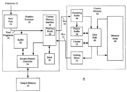
 
Xmas - in this diagram:

b3d16.gif


I believe that the 256GB/s "effective bandwidth" is what happens between the Data Path 48 and the Memory Array 46.

It is these two components that are involved when a pixel is blended, or a z-test is performed or when AA samples are filtered.

The bus represented by 30/32 appears to be capable of an effective 32GB/s (2 quads read or write per clock). Whether it's bi-directional (actual 64GB/s) is unclear. But this data is in compressed form, so the actual bandwidth here is unknown...

My understanding of the patent is that AA samples are re-calculated by the Sample Memory Controller, 24. So when a new fragment representing a triangle edge is overlayed on a pixel that represents an existing triangle edge (e.g. two triangles that share an edge), it is the Sample Memory Controller that evaluates the existing pixel (fetched by the Data Path 48) and determines how to recalculate the AA sample set, updating it in Sample Memory 25.

So, not all of the AA workload is carried out within the Data Path 48.

Jawed
 
Jaws, on another thread, has just pointed out that the read bandwidth 32 is only half the write bandwidth 30. :oops:

Jawed
 
This eDRAM sounds somewhat similar to Mitsubishi's 3D-RAM which was used by E&S and Sun ages ago. That memory had some logic on-board to handle blending and Z-compare.

Per, Sweden
 
I wonder how (if?) they implement early Z test with this kind of configuration. If Z and stencil test is performed inside the enhanced memory chip early Z would require a feedback bus to send back the per quad masks with the result of the tests. Hierarchical Z also requires feedback from the Z test. If I'm correct in my assumptions and readings of ATI patents and the old HOT3D presentation the per block representative Z value for the HZ is calculated when Z cache lines are evicted and compressed.

Not implementing early Z and/or Hierarchical Z would be a very bad idea on terms of utilization of the shading power. Every fragment that can be removed before shading counts a lot.

Special video memory (VRAM) with blending or other acceleration features is a very old history, however I didn't even bothered much to study it as the trend lately has been to use common DRAM. The most extreme implementation of this approach could be something like the Pixel Plane architecture where each pixel had the whole hardware to perform all the tasks from rasterization (but only after setup, geometry is also performed in the CPU or another processor) to blend and color write.
 
Per B said:
This eDRAM sounds somewhat similar to Mitsubishi's 3D-RAM which was used by E&S and Sun ages ago. That memory had some logic on-board to handle blending and Z-compare.

Per, Sweden


That's how i understand it too.

So in the end the Xenon-GPU is just an upgraded PS2-GS with 10MB + a shader-core attached on the side. :D

Well not really, but IMHO it combines the advantages of the eDRAM-enhanced blending-monster GS with an sea of ALU's for very high performance shading (textures, pixel-shaders, vertex-shading ).
 
RoOoBo said:
I wonder how (if?) they implement early Z test with this kind of configuration. If Z and stencil test is performed inside the enhanced memory chip early Z would require a feedback bus to send back the per quad masks with the result of the tests. Hierarchical Z also requires feedback from the Z test. If I'm correct in my assumptions and readings of ATI patents and the old HOT3D presentation the per block representative Z value for the HZ is calculated when Z cache lines are evicted and compressed.
HierZ doesn't need feedback from the Z test. You simply store the farthest Z value per tile. If the incoming tile is beyond that, it is discarded. If it is half-filled and in front, it is accepted. If it is filled and in front, its farthest Z value is written to the tile.
If any other tests are enabled (alpha, stencil, kill), writes to the tile are disabled. If the Z comparison changes, hierZ is disabled.
 
Back
Top