
You are using an out of date browser. It may not display this or other websites correctly.
You should upgrade or use an alternative browser.
You should upgrade or use an alternative browser.
AMD's new G34 socket on a sketch...
- Thread starter fellix
- Start date
Quad channel RAM and 4 HT links should be interesting.
The new socket's time frame unfortunately also gives us a pretty good idea of the magnitude of the change or rather non-change in AMD's chips we can expect until 2010.
That Magny-Cours and its ilk will be coming out on the new socket also reinforces my earlier impression that Bulldozer is really pushed out. There would be no point in introducing the 12 core chip if its sucessor was coming out soon after.
Cache capacities per-core will also not change much either. AMD's lackluster cache density may very well be the rule for years to come.
AMD needs to use the same cache design. (SOI was blamed for Barcelona's L3 density, and it hasn't improved for Shanghai).The L3 array is where more work can be done, as for now AMD is just recycling the L2 SRAM design for the L3.
It doesn't appear to be the case, looking at the per-chip cache capacities, that it's only doing it "for now".
The L3's density not improving over the L2 has not changed for Barcelona to Shanghai, and the numbers don't indicate a significant change for anything in the next two years.
Blazkowicz
Legend
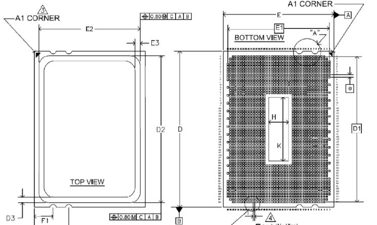
AMD is working on a new CPU architecture codenamed 'Bulldozer'. Derivatives include monolithic 8-core and 12-core processors. The 12-core processor is now codenamed Magny-Cours, the 8-core part is called Sao Paulo. These processors could feature four parallel HyperTransport 3.0 interconnects, upto 12 MB of L3 cache and 512 KB L2 cache per core. It's known that AMD could be working on quad-channel DDR3 (both registered DDR3 under G3MX and unregistered). Socket G34 seems to have 1,974 pins.
aren't they mixing things up? Sao Paulo should be 6-core and Magny-Cours a CPU made of two Sao Paulo dies (as core2quad and pentium D 9xx)
I wonder how will a 12 core Magny-Cours stack up against a 32 core Larrabee
Why would it? Larrabee is a graphics product that just so happens to be GPGPU (and x86) capable. Single-thread performance will be *attrocious* compared to even current x86 processors, let alone what's to come at the time of Larrabee's release.
One step closer to slot-A?
Sort of makes AMD's HT co-processor concept seem not-so-bad now, eh?
Oh my gods, did anyone else notice that it's not square?
I've seen comments that a rectangular socket helps with routing, since signal IOs near the center don't have to route through as many other pads to get out of the socket.
I'm not a board designer, so I don't know.
Going quad-channel DDR3 would seem to support it though, since the extra channels and additional HT links helped balloon the pin count 700+ pins.
Routing all those memory channels to one side would be easier if that side were longer.
I'm not a board designer, so I don't know.
Going quad-channel DDR3 would seem to support it though, since the extra channels and additional HT links helped balloon the pin count 700+ pins.
Routing all those memory channels to one side would be easier if that side were longer.
Why would it? Larrabee is a graphics product that just so happens to be GPGPU (and x86) capable. Single-thread performance will be *attrocious* compared to even current x86 processors, let alone what's to come at the time of Larrabee's release.
Why would I want to compare single-threaded performance? You would think I am talking about those x86 GPGPU programs. And no I think larrabee is more like a general purpose processing unit just happens to have graphics functionalities attached to it.
Last edited by a moderator:
Why would I want to compare single-threaded performance? You would think I am talking about those x86 GPGPU programs. And no I think larrabee is more like a general purpose processing unit just happens to have graphics functionalities attached to it.
Yeah, all what - one of them (FAH GPU client)?
Show me the apps, then we'll talk perf. Until then, no useful perf. comparo can be made (outside of theoreticals and ONE app).
Note: I realize there is more than one GPGPU app in existence, but we are talking about consumer hardware here, and these multiple apps exist outside of the consumer space.
Show me the apps, then we'll talk perf.
I agree we need apps for comparison but we are talking about vapour-ware here...
Last edited by a moderator:
Similar threads
- Replies
- 16
- Views
- 1K
- Replies
- 68
- Views
- 5K
- Replies
- 9
- Views
- 702
- Replies
- 21
- Views
- 2K