AMD CDNA: MI300 & MI400 (Analysis, Speculation and Rumors in 2024)

Their testing doesn't make sense to me. Why are they using ZeRO-Inference (optimised for running huge models with weights stored outside GPU DRAM) on a 8xMI300X system with 1536GB of GPU memory? How are they managing to get OOM on a 8xH100 system at a batch size of 16 for a 170B model? That doesn't mean MI300X is good or bad; just that those specific tests are useless.

We should start a new MI300X(/MI400?) thread, it's worth discussing but NOT in the same thread as Blackwell, that will just inevitably lead to drama and low signal-to-noise. A lot of posts in this thread discuss both Blackwell and AMD so I'm not sure it works to just move all of them into a new thread unfortunately...
 
There are also some updates to testing in their blog.

Agreed about the OOM and is still present in updated tests.
 
We should start a new MI300X(/MI400?) thread, it's worth discussing but NOT in the same thread as Blackwell, that will just inevitably lead to drama and low signal-to-noise. A lot of posts in this thread discuss both Blackwell and AMD so I'm not sure it works to just move all of them into a new thread unfortunately...
Agreed. I thought there might be an MI300X thread but maybe it's collapsed into the CDNA Discussion thread?
 
Their testing doesn't make sense to me. Why are they using ZeRO-Inference (optimised for running huge models with weights stored outside GPU DRAM) on a 8xMI300X system with 1536GB of GPU memory? How are they managing to get OOM on a 8xH100 system at a batch size of 16 for a 170B model? That doesn't mean MI300X is good or bad; just that those specific tests are useless.
Looking around the site they offer only AMD solutions. No mention of where the 8xH100 results were derived or whether it was optimized.
 
Looking around the site they offer only AMD solutions. No mention of where the 8xH100 results were derived or whether it was optimized.
They claim they'll also have H100s soon so presumably they have their own 8xH100 already. But that doesn't matter, the whole setup is weird and doesn't tell us much about other environments unfortunately.

Fundamentally though: if this article is right and AMD is selling MI300X for $15K (or ~$10K for MS) versus NVIDIA's $30K for H100 80GB (and probably less for MS too, maybe $20K?), while they have 1.75x as much HBM3 bandwidth and 4-5X as much L3 cache, it's obvious that AMD has much better perf/$ than H100 for bandwidth-limited workloads like "LLM inference at low/medium latency with limited batch sizes" if the frameworks aren't too badly unoptimised for AMD (which will get better over time). In practice they won't hit achieve that performance due to frameworks and the manufacturing cost for AMD is probably ~2x H100 80GB, but it's still a very attractice first product for the inference market.

BTW - NVIDIA claimed in their latest earnings call that inference was currently ~40% of their AI revenue vs ~60% for training, but that was only their best estimate as it's hard to know for sure (and GPUs could presumably be bought for training then reused for inference the year after etc...). I think it's fair to say that inference doesn't currently dwarf training yet, it probably will sooner rather than later, but right now an awful lot of money is still going into training clusters because everyone is desperately trying to achieve the next great breakthrough. I would only expect NVIDIA to lose noticeable market share in inference rather than in training short-term, so a lot depends on how quickly the mix changes between training vs inference.
 
I'm not an expert here, but I'd imagine that regarding to inference vs training, people are more likely to focus on cost and efficiency when doing inference than training. When doing training, people are probably more willing to pay a premium for faster and more capable hardwares because there can be time constrain or people might want to build larger models etc. However, when doing inference it's more important to run it as cheap as possible because you'll be serving a lot of requests and that's generally what you charge your customers for. So if you can do it cheaper you can charge your customers less (more competitive) or you can make more money.

It's also quite obvious that running inference locally ("edge") is going to be huge. This is actually where those custom-built accelerators are going to shine.
 
Fundamentally though: if this article is right and AMD is selling MI300X for $15K (or ~$10K for MS) versus NVIDIA's $30K for H100 80GB (and probably less for MS too, maybe $20K?),
It's Citi, they don't know anything AMD.
Absolute mouthbreathers.
They had like $20 $AMD target for eons and only recently adjusted it a bit below $100.

Either way the pricing is ~$19k for MI300 and ~$22k for H100 but it doesn't quite hold this static since neither side likes losing MSS at key customers.
 
Is there any info on how work is allocated across MI300 chiplets such that the whole setup presents as a single compute device? Is there a global hardware work distributor on one of the dies or is it all managed by the host CPU & driver?
 
Is there any info on how work is allocated across MI300 chiplets such that the whole setup presents as a single compute device? Is there a global hardware work distributor on one of the dies or is it all managed by the host CPU & driver?
each XCD has I think 1 HWS and 4 ACEs so it's just a very obese design of 8 HWS and 32 ACEs for the full GPU.
Only graphics ring on AMD is reliant on centralised CP. For now, anyway.
 
Last edited:

each XCD has I think 1 HWS and 4 ACEs so it's just a very obese design of 8 HWS and 32 ACEs for the full GPU.
Only graphics ring on AMD is reliant on centralised CP. For now, anyway.

Thanks but I’m not sure how the article is relevant. It seems to be addressing off package / inter-node communication. My question was more about how work is distributed across the multiple XCDs on a single package.

Is the driver deciding which HWS on which XCD processes a given compute workgroup? I had assumed that allocation was done in hardware on monolithic chips.
 
Thanks but I’m not sure how the article is relevant.
just a news post.
My question was more about how work is distributed across the multiple XCDs on a single package.
The same it's scheduled across multiple SEs.
Is the driver deciding which HWS on which XCD processes a given compute workgroup?
You just see a bunch of compute queues and that's all. You dispatch kernels. It works.
Don't remember if the h/w is round-robin or something smarter.
I had assumed that allocation was done in hardware on monolithic chips.
Works the same on MI300.
You just have more queues.
 
just a news post.

The same it's scheduled across multiple SEs.

You just see a bunch of compute queues and that's all. You dispatch kernels. It works.
Don't remember if the h/w is round-robin or something smarter.

Works the same on MI300.
You just have more queues.
But where the hw schedule is located ?
 
But where the hw schedule is located ?
Across all dies.
Compute hasn't had a singular unified scheduler queue since Tahiti.
All driver sees is moar queues to launch kernels at.
You launch kernels, it dispatches packets to HWS and there you go.
You already had 2 HWS per part. Now you have 8. Not much changed?
 
Across all dies.
Compute hasn't had a singular unified scheduler queue since Tahiti.
All driver sees is moar queues to launch kernels at.
You launch kernels, it dispatches packets to HWS and there you go.
You already had 2 HWS per part. Now you have 8. Not much changed?

Oh interesting so allocation of workgroups to HWS is done host side. That makes sense.

Presumably the knowledge of which IF node contains which queue/HWS is baked into the firmware.
 
Last edited:
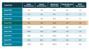
Couple things looking over the whitepaper again, they doubled the vector (CU) FP32 rate? Now the same as matrix FP32/64 rates, after last gen going full rate FP64. They don't specifically say what changed but this is as close as it gets, more VOPD shenanigans? Don't think I've seen it mentioned anywhere else:

While the compute units are architecturally similar to those in AMD
CDNA™ 2, they have been comprehensively improved with major changes throughout the core to exploit
greater parallelism at nearly every level and in many cases doubling or even quadrupling the performance per
CU for vector and matrix workloads.

These numbers don't include sparsity either for the matrix rates so you can double the TF32 numbers and below, although they are added in a latter table

amd mi300x specs HL PNG.png
 
Oh interesting so allocation of workgroups to HWS is done host side. That makes sense.
HWS and ACE have known to be firmware running on embedded cores for a few generations, dated back to at least “HWS” was introduced (Polaris?). You can also find clear signs of this in AMDKFD. Worth noting as well that the shader dispatch is a separate facility, multiplexing commands from ACEs as well as the graphics front-end.

Given that GFX940 can be configured as a single agent crossing multiple XCDs, I would assume ACEs can break down and launch kernels against both local and remote XCD shader dispatches. Otherwise, it won’t be able to present a truly “single agent” model, since each queue would be forced to accept only CU affinity that slots into exactly one XCD.

(Note: This doesn’t contradict “having more queues” up thread. HWS is responsible for scheduling userspace HSA queues from kernel driver “over-subscribable” runlists onto ACE hardware queues. So in theory, while a single agent GFX940 configuration can have only 1 HWS by nature, it could have all the ACE queue pipes across all XCDs at its disposal.)
 
Last edited:
Back
Top