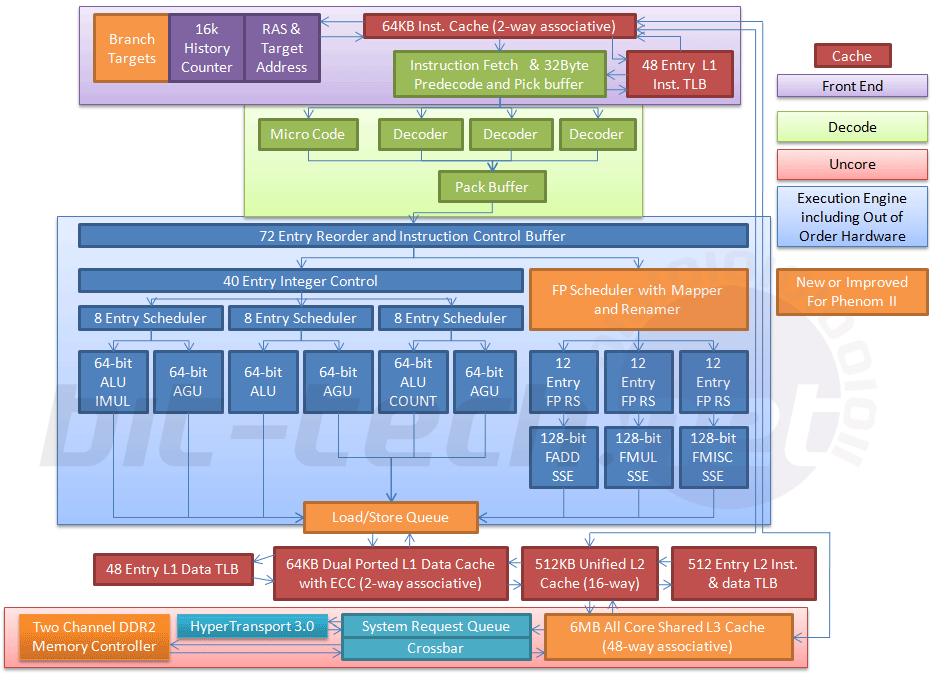
AMD Bulldozer Core Patent Diagrams

Even with improved load/store and other tweaks, I have a hard time to believe they can make up for the loss of the third pipe - might be close though.
Certainly however, multithreaded performance should be much better than K8 (without making the chip too big, multithreaded performance per transistor (or per die area) should be higher hence more cores at the same die size (or in the same power envelope)).

Intel's architecure also only has two issue ports to ALUs and I'm sure we can agree it does quite well.

Bulldozer brings AMD on par with Intel, microarchitecture-wise. The question now is, how fast does it clock.

Cheers
 
Intel's architecure also only has two issue ports to ALUs and I'm sure we can agree it does quite well.
Nehalem (just as Core 2, but not Yonah) has 3 integer pipelines and can consequently issue 3 integer ops per clock (though the issue ports are shared with fp issue).
 
if you look at dresdenboys blog there are a couple of new entires both about int performace. There is a link to an AMDzone thread which has details from the presentation that wasn't in any slides.

There is also a post from usenet of someone who claimed to have come up with the overall uarch idea over 10 years ago and he had a project based on it 6 or so years ago when working at AMD that got cancelled, he then talks about possible further interations of the design.
 
Hmm cool, this is similar to my interpretation, namely the size of the FP units is too big/utilisation too low to properly justify a full dedicated FP unit per int core -> share one between two relatively low cost int cores.
in some ways, it is the advent of expensve FP,
like Bulldozer's 2 sets of 128 bit, 4x32 bit, FMAs, that justify integer
MCMT: the FP is so big that the overhead of replicating the integer
cluster, including the OOO logic, is a drop in the bucket.

It seemed perfectly logical that they'd trim the int cores a bit to not be adding too many transistors but wow, 2* 4 wide is pretty extreme :oops:


& here we have an AMD guy trying to clarify some terminology
A Bulldozer module has the following: 2 Integer cores. One 256-bit shared FPU (that can be addressed as a single 256-bit unit or 2 128-bit units per cycle). Shared front end. Shared L2 cache.

Each Bulldozer module is seen by the OS as 2 cores. The OS does not see a module, only cores.

Interlagos has 8 Bulldozer modules for a total of 16 cores.

Valencia has 4 Bulldozer modules for a total of 8 cores.
 
Last edited by a moderator:
The only bad thing is that some guys I know at AMD say that Bulldozer is
not really all that great a product, but is shipping just because AMD
needs a model refresh. "Sometimes you just gotta ship what you got."

http://groups.google.com/group/comp...fa0b8b07/3cd3bfa93b736a56?q=#3cd3bfa93b736a56

An interesting quote from someone who probably has enough connections to get a feel for the general sentiment regarding this product. Maybe it's not so great compared to some revised version of the core coming later on and they had to scrap some massive performance enhancing features to push this thing out the door. Still a little dissappointing considering how late this thing is.

so that means it can do one four dimensional 64bit FMAC per clock?
is it matching the sandy bridge there?

http://www.amdzone.com/phpbb3/viewtopic.php?f=52&t=137095&start=25#p171265

That post seems to indicate that 256bit execution suffers no penalty when compared with legacy 128bit instructions. Each Bulldozer module (2 integer cores + 2 128-bit FMACs) seems like it's roughly a match for each Sandybridge core.
 
http://groups.google.com/group/comp...fa0b8b07/3cd3bfa93b736a56?q=#3cd3bfa93b736a56

An interesting quote from someone who probably has enough connections to get a feel for the general sentiment regarding this product. Maybe it's not so great compared to some revised version of the core coming later on and they had to scrap some massive performance enhancing features to push this thing out the door. Still a little dissappointing considering how late this thing is.

he left AMD 5 years ago, he said himself that it likely has lots of new ideas in it that he isn't aware of. Who knows what he knows personality clashes can make people say just about anything.
 
he left AMD 5 years ago, he said himself that it likely has lots of new ideas in it that he isn't aware of. Who knows what he knows personality clashes can make people say just about anything.

That's entirely possible, and judging from the performance projections, it shouldn't be too shabby if they hit their clock targets. I'd like to see what they put in place of the FPUs in the future.
 
Nehalem (just as Core 2, but not Yonah) has 3 integer pipelines and can consequently issue 3 integer ops per clock (though the issue ports are shared with fp issue).

True, it has three ALUs. I don't think the sharing the issue port with fp is an issue. What is an issue is that the port 1 ALU is also used for LEAs, the chance of hitting an instruction mix of 3 int alu ops and no loads on x86 over a sustained number of cycles has a very low order of probability.

Assuming the load and store pipes in bulldozer has their own AGUs, the amount of resources is similar to core 2/i5/i7.

Cheers
 
Last edited by a moderator:
Nehalem has 3*128bit FP per core?! But it executes either 3* int or 3* FP at a time?
I never realised that somehow & its completely the opposite direction that Bulldozer has gone :oops:

Core 2s and forward can fetch, decode and inject into the ROB, up to 4 instructions per cycle. It can issues up to 6 instructions for execution per cycle. It can retire up to 4 instructions per cycle.

The issue restrictions reflect common instruction mixes. You basically always need loads and stores. What you do with the values from those loads and stores depends on your workload, int or fp intensive, which is why overloading the issue ports works out.

Cheers
 
some more floating point fun,

http://citavia.blog.de/

its amazing what people can find when they know where to look :p

It doesn't make a lot of sense, IMO. The purpose of fusing multiply and add is to cut down the number of results that has to be broadcast/forwarded and thus cutting down on the bypass network (or number of result busses).

I could imagine the floating point unit detect pairs of FMULS and FADDs and fusing them to FMAC with intermediate rounding (ie. results are identical) to save instruction entries in the ROB/reservation stations as well as reducing result bandwidth needs. The FADD in a FMAC is essentially free from a logic/area point of view.

So you would have two units: FMAC that does FMACs (FMADDs), FMULs and FADDs while the other unit just does FADD.

Cheers
 
Last edited by a moderator:
my understanding of this at a technical level is flaky at very best but i did read

http://users.ece.utexas.edu/~quinnell/Research/Bridged Floating-Point Fused Multiply-Add Design.pdf from beggining to end.

from what i can see it sacrifices some latency and higher power for FMA to allow inderpendant execution of regular operands on the adders and mul.

The bridge architecture is 30% to 70% faster and 50% to 70% lower in power consumption than a classic fused multiply-add unit when executing single-unit instructions. The bridge fused multiply-add architecture is about 50% larger than a classic fused multiply-add unit.

it seems to be a trade off of raw FMAC performace vs "legacy" performace.

6. CONCLUSION
A new architecture for the design and implementation of a fused multiply-add unit with high
performance stand-alone floating-point addition and multiplication instructions has been
presented. The bridge fused multiply-add architecture implements a fused multiply-add
instruction by adding a “bridge” in between a standard floating-point adder and floating-point
multiplier, all while re-using components from both to minimize the implementation costs. The
bridge fused multiply-add unit shows almost identical latency and power consumption for
addition and multiplication instructions as compared to typical stand-alone floating-point
arithmetic units at the cost of increased area and a higher-performance fused multiply-add
operation as compared to the stand-alone units. It does exhibit lower-performance for the fused
multiply-add operation as compared to the classic fused multiply-add unit.
 
Chaps

Apologies if this low level query has already been covered.

We know that a single Bulldozer "unit" has dual integer resources and appears as two logical processors to the OS. But it also has a single shared FP resource.

Hence my question is - what happens when the OS schedules two FP threads on a single Bulldozer unit?
 
Hence my question is - what happens when the OS schedules two FP threads on a single Bulldozer unit?
I guess the single FP scheduler would just reorder / issue as it sees fit. That should actually help with utilization I guess, since you have no data dependencies between the two threads so more possibility for reordering in case of data hazards (and since there are two 128-bit fmac units it might even be possible to issue a sse instruction from one thread and one from another at the same time). In that sense I guess it would be like hyperthreading, with probably just doubled register file. I'm sure though in practice it's a bit more complicated than that, but I can't see any major problems.
 
I guess the single FP scheduler would just reorder / issue as it sees fit. That should actually help with utilization I guess, since you have no data dependencies between the two threads so more possibility for reordering in case of data hazards (and since there are two 128-bit fmac units it might even be possible to issue a sse instruction from one thread and one from another at the same time). In that sense I guess it would be like hyperthreading, with probably just doubled register file. I'm sure though in practice it's a bit more complicated than that, but I can't see any major problems.

I think you're right. And since fp instructions with memory operands won't get injected into the FPU until the int-box has loaded the memory operand, the scheduler/ROB in the FPU doesn't have to deal with memory latencies, only instruction latencies. This could allow a quite wide internal structure for the same timing and power constraints.

I could image a worst case instruction latency of 16 cycles (FDIV), a four-wide FPU would then need a 64-entry ROB.

Cheers
 
I was wondering the other question - how will one thread be able to use the whole fpu, how can the OS schedule for that ; does that require using AVX instructions?
 
I was wondering the other question - how will one thread be able to use the whole fpu, how can the OS schedule for that ; does that require using AVX instructions?
There shouldn't be any difference if one or two threads use FPU instructions, the FPU scheduler could hardly care. The scheduler will try to find instructions with no data dependencies and schedule them on the two fmac units (I think we're missing some details here what those units really can do and if they are symmetrical). If you have AVX instructions then it should obviously be easier because they can just always use both fmac units (or do avx instructions get issued twice on one fmac unit? In either case I think some magic is needed to make it work, since I guess there are instructions to shuffle operands around from the lower half to the upper half of the bits and similar things).
If you actually want to get the peak flops number, this would require fmac instructions, which avx apparently lacks, but this is again completely independent from the number of threads.
 
oh well, some reading to understand about the instruction sets :
http://en.wikipedia.org/wiki/FMA_instruction_set
http://en.wikipedia.org/wiki/SSE5
http://en.wikipedia.org/wiki/Advanced_Vector_Extensions

this has cleared confusion for me. Basically, AVX is extensible, and Intel will support FMA later, likely on the sandy bridge shrink.
AMD has moved its SSE5 extensions to AVX, including FMA. off course both FMA instructions are different, to spice things a bit, but future CPU may suport both (read link for more details) ; AMD should support both.
 
Back
Top