That's a mockup made before the real chip was released. The die size is very off.
You are using an out of date browser. It may not display this or other websites correctly.
You should upgrade or use an alternative browser.
You should upgrade or use an alternative browser.
I think there's a die-shot of Llano K10.5 core with it's L2 cache and exact dimensions (area) floating in the web. If this Orochi part uses the same L2 SRAM cell size/structure (both CPUs are 32nm), it will be easy to figure out a loose die area number of the whole chip.The L3 looks like it is segmented between modules, so there could be some variable latency between a local tile and a non-local tile. Hopefully that means there is better average latency, given that Bulldozer's L2 has latencies closer to an L3 already.
It looks like a more square die than Istanbul, and one side is able to take the full length of the DDR interface.
That is longer than the analagous side of an Istanbul chip, which had to run the interface around two corners.
If the length of that side is enough to get an idea of the scale, Orochi seems likely to be larger than Westmere, which is 248mm2.
I haven't found a good number for the dimensions for Istanbul's interface pads, particularly if they were straightened out.
Jawed
Legend
Blimey I thought the artist impression bit was just the labelling.That's a mockup made before the real chip was released. The die size is very off.
I think Hans Devries had a bit of a laugh about that. I believe this was just a bit of speculation that some web sites ran with as actual die shots. Istanbul is roughly 346 mm2.
It seems that Orochi's "long" side has the DDR pads, while Istanbul had the "short" side and part of the long sides devoted to the pads.
It's roughly third longer than it is wide, going by the pic.
The question is whether the interface at full length measures on the order of 18mm. Anything in that range is going to put Orochi at or over Westmere.
Perhaps I can find the time to track down and compare Llano's L2 area, given the uncertainty of the pad length.
I counted 9 data pad structures (8*DQ + 1*ECC), so it appears to be complete.The question is whether the interface at full length measures on the order of 18mm.
A clearer shot, and more, is in the PDF of the presentation.
http://phx.corporate-ir.net/External.File?item=UGFyZW50SUQ9NjExNDN8Q2hpbGRJRD0tMXxUeXBlPTM=&t=1
http://phx.corporate-ir.net/External.File?item=UGFyZW50SUQ9NjExNDN8Q2hpbGRJRD0tMXxUeXBlPTM=&t=1
I think the top and bottom are flipped. The left side cores are likely allowed to be somewhat offset because the memory controller/northbridge is probably bulking up the center of the die on the right, and has no reason to extend all the way across the chip.
There was a similar offset for the hexacore chips AMD has out right now, the additional two cores appear a little different because they are slightly closer to each other and so offset from the other four. It does seem to indicate the "axis" of Orochi is different from Istanbul's.
There's a lot of seemingly empty space, probably power gates and less fancy data paths.
Look at the upper two L2 arrays -- I think those are resized on the horizontal axis with lots of re-sampling artifacts visible as a result. I remember an AMD representative saying that they had an intention to photochop crucial parts of the BD die-shot(s) for their future presentations.
Look at the upper two L2 arrays -- I think those are resized on the horizontal axis with lots of re-sampling artifacts visible as a result. I remember an AMD representative saying that they had an intention to photochop crucial parts of the BD die-shot(s) for their future presentations.
They messed with the lower two arrays as well, unless variably-sized cache arrays are the new fad.
I'm now more curious about whether they did anything to hack up the less glamorous parts of the die, such as the L3 or any of the IO sections.
Jawed
Legend
http://www.xtremesystems.org/forums/showpost.php?p=4534641&postcount=860
8-core Orochi die. Heavily photoshopped. We don't release the final shots until launch.
Looks like AMD photochop goons messed up not only the CPU cores, but a part of IMC/NB area:

The structures, highlighted in the green rectangle, have been clone-stamped over and over again with patterns from the IMC/NB to the right side, to fill out (completely conceal) something equally important to the cores.
I can only speculate, that this is an L3 directory cache and routing logic, if we are to believe the four L3 partitions are private to each "module".
I am less sure that the L3 is really subdivided the way that the picture depicts. There is a lot of apparent dead space between the banks, and a lot of dead space in general in the middle.
For instance, if the L3 quadrants were linked to their neighboring module, why so much margin between them and the cores?
The real irony would be that if we just counted the area devoted to the L3 arrays, they would appear unusually dense if we assumed the L3 had 8MiB of capacity.
It seems AMD has cloned a lot of the brown border, perhaps to hide the physical size of the L3.
It would seem cruely ironic that for all the trumpeting of die space savings by merging cores, AMD then ruined the density of the rest of the chip.
For their sake, I'd hope they also edited the IO sections, or less likely they've significantly improved the physical size of those features. Orochi becomes signficantly less impressive versus Westmere the closer it gets to 300mm2 and above.
hoom
Veteran
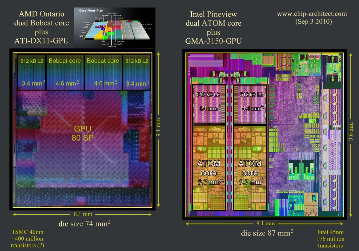
Now there is some more detail on Bobcat: 9W for Ontario & 18W for higher clocked Zacate core. No clocks given though.
There is a photo of the die with metal layers, handily matched up with Pinetrail by Hans de Vries

How did they get Bobcat core to be less than half the area of Atom???
I've seen it claimed that TSMC 40nm is just a marketing differentiation vs 45nm but if he's highlighted the right bits for the 512KB L2 & the scaling is right then clearly they do have legitimate claim to the smaller scale.
Regarding the Bulldozer shot, Nehalem & onwards partitioned the L3, so its not particularly surprising to see AMD do it too.
The 'gaps' seems to be a fundamental difference between AMD & Intel.
I'm thinking maybe AMD is using parallel internal busses while Intel has switched to a much thinner Serial tech?
But I thought busses etc ran through the metal layers, so why would there be such a footprint on the die?
There are a bunch of actual Istanbul die shots at http://www.pcgameshardware.com/aid,...cle&image_id=1068226&article_id=682381&page=1
There is a photo of the die with metal layers, handily matched up with Pinetrail by Hans de Vries

How did they get Bobcat core to be less than half the area of Atom???
I've seen it claimed that TSMC 40nm is just a marketing differentiation vs 45nm but if he's highlighted the right bits for the 512KB L2 & the scaling is right then clearly they do have legitimate claim to the smaller scale.
Regarding the Bulldozer shot, Nehalem & onwards partitioned the L3, so its not particularly surprising to see AMD do it too.
The 'gaps' seems to be a fundamental difference between AMD & Intel.
I'm thinking maybe AMD is using parallel internal busses while Intel has switched to a much thinner Serial tech?
But I thought busses etc ran through the metal layers, so why would there be such a footprint on the die?
There are a bunch of actual Istanbul die shots at http://www.pcgameshardware.com/aid,...cle&image_id=1068226&article_id=682381&page=1
Last edited by a moderator:
Now there is some more detail on Bobcat: 9W for Ontario & 18W for higher clocked Zacate core. No clocks given though.
There is a photo of the die with metal layers, handily matched up with Pinetrail by Hans de Vries

How did they get Bobcat core to be less than half the area of Atom???
I've seen it claimed that TSMC 40nm is just a marketing differentiation vs 45nm but if he's highlighted the right bits for the 512KB L2 & the scaling is right then clearly they do have legitimate claim to the smaller scale.
Regarding the Bulldozer shot, Nehalem & onwards partitioned the L3, so its not particularly surprising to see AMD do it too.
The 'gaps' seems to be a fundamental difference between AMD & Intel.
I'm thinking maybe AMD is using parallel internal busses while Intel has switched to a much thinner Serial tech?
But I thought busses etc ran through the metal layers, so why would there be such a footprint on the die?
There are a bunch of actual Istanbul die shots at http://www.pcgameshardware.com/aid,...cle&image_id=1068226&article_id=682381&page=1
This area distribution IS wrong.


