Speculation and Rumors: Nvidia Blackwell ...

  • Thread starter Deleted member 2197
  • Start date
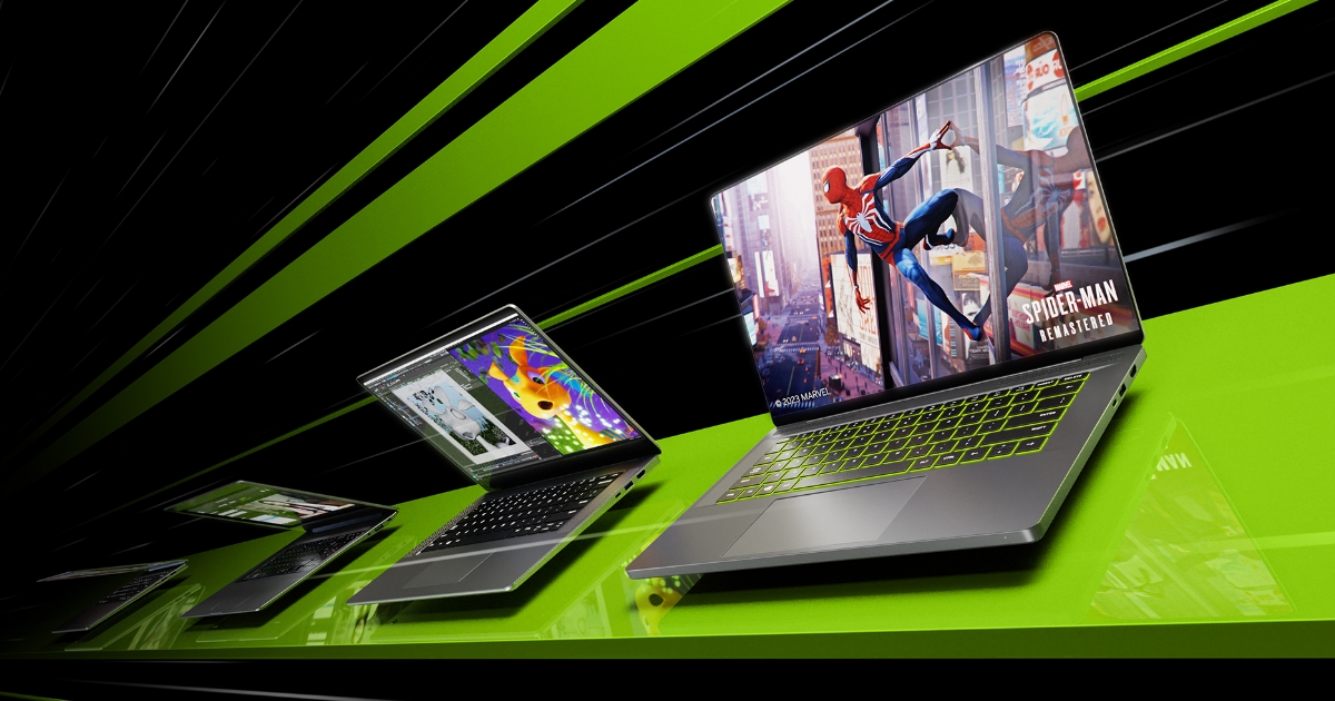
They aren't saying it pulls 140W continuously, nor that 140W is the limit everyone uses. THey're saying (and they're correct) the SKU permits limiting the GPU across a range of power, from 35W (I didn't look it up, I'm trusting pcchen on this number) to 140W. The actual power limit profile is determined by the manufacturer of the laptop and programmed into the firmware. This power limit is typically immutable, so the end user can't up the power slider in MSI Afterburner on a laptop as they might on a desktop part.

The new SKU apparently caps that range to 115W, therein lies the "interesting" story apparently.

Hope that clears it up.

Of course it’s not continuous. We’re comparing TGPs. As long as they’re comparing peak to peak there’s no problem. It’s not clear from the article that 115W is the peak TGP for the 5060M though.
 
It appears 140W refers to the 115W TGP configuration plus NVIDIA"s "Dynamic Boost 2.0" which allows up to another 25W, as a function of removing power from the CPU, in cases where chip thermals permit the extra power consumption. Both the configuration of the base SKU (eg 45W, 80W, 115W) plus support for Dynamic Boost 2.0 must both be baked into the laptop firmware to permit this behavior, which is why there are laptops in the wild with "140W" rated 4060's.

EDIT: Totally beaten to the punch by @DegustatoR :)
 
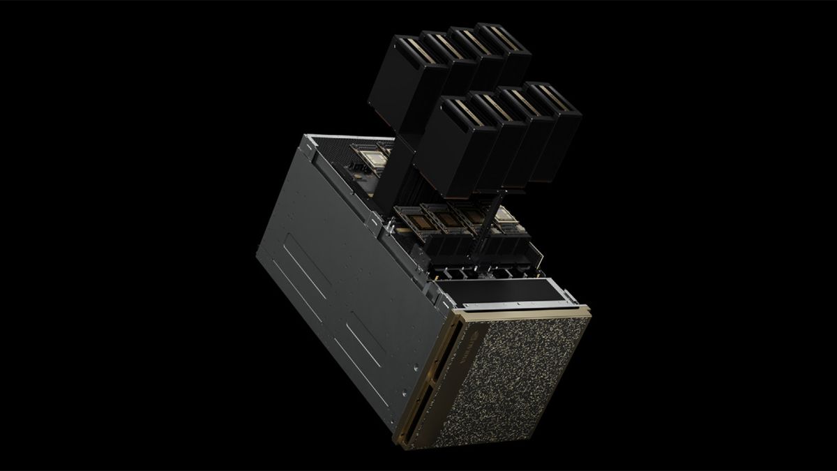
The Blackwell Hot Chips presentation was a bit of a nothing burger, very light on details… except…

They confirmed 2x Tensor Core flops per SM *and* higher peak clocks. But the peak flops per die for B200 is nowhere near 2x H100 (it’s obviously >2x when considering both dies).

That very strongly implies there are fewer but bigger SMs, possibly with 256 FP32 FMAs per SM, which might also hint at larger architectural changes overall.

Yes, i was looking forward to it, as they didn't show a whitepaper and then there was nothing. Seriously, for such an architecture presentation they should remove nvidia from the Hot Chips main presentations.
 
Yes, i was looking forward to it, as they didn't show a whitepaper and then there was nothing. Seriously, for such an architecture presentation they should remove nvidia from the Hot Chips main presentations.

Nvidia has gotten absolutely trash at presentations recently, a recent programming one was just an hour plus long nvidia ad with no information whatsoever. But that was a sponsored talk so, sure waste it on doing a useless ad, I suppose.

This feels the tiniest bit criminal, considering how objective the Hot Chips presentation committee is supposed to be, how much it costs to attend, and how high the competition to get papers into the conference is. I'd kinda like to see Nvidia banned from Hot Chips for a few years for wasting peoples time and money so flagrantly.
 
When was the last time Nvidia ever gave out any real architectural details via presentation or white paper? Everything I have been able to find going back to at least Pascal has never had more than marketing beats.
 
NVIDIA also had 3 presentations for the Tutorials day that felt reasonably informative to me; not super detailed, but given the primary audience at Hot chips aren't experts in liquid cooling or LLMs, they were pretty good imo.

For GPU architectures, I think the amount of information in their Hot Chips presentation has been going down every generation since Volta, where they talked about some previously undisclosed details of the SM microarchitecture, see slides 9 to 12: https://old.hotchips.org/wp-content...HC29.21.132-Volta-Choquette-NVIDIA-Final3.pdf

Blackwell will probably be the highest revenue chip of 2025, so the committee can't really refuse a presentation about it even if NVIDIA doesn't want to (/isn't ready to) talk about the architecture. I hope NVIDIA will eventually publish more details but I’m not super optimistic, we’ll probably have to figure everything out with microbenchmarks.
 
MLPerf Inference 4.1 results are out, including B200, H200 and MI300X!
MI300X results is only for LIama 2 test, which isn't a good showing really, if AMD has more confidence they should've submitted results for all tests. H100 is on par with MI300X here, while H200 is 40% faster, B200 is 4x faster than H100/MI300X.
 
Last edited:
MI300X results is only for LIama 2 test, which isn't a good showing really, if AMD has more confidence they should've submitted results for all tests. H100 is on par with MI300X here, while H200 is 40% faster, B200 is 4x faster than H100/MI300X.
ML perf is a bit, questionable. Basically don't believe that it's some objective benchmark even though it's claimed as such.

Benchmarking inference and training is a big question right now, one made fundamentally unsound even in theory by the fact that optimization can bring a lot of performance gains. Which means the same hardware can deliver different results month to month, which obviously isn't very conducive to the very idea of having a "benchmark". Leave alone the fact that new model version also seem to release incredibly quickly.

I understand the desire for comparative data. But there's just not a good metric for such right now. Treating MLPerf as much more than PR seems a mistake at the moment, much as might be desired otherwise.
 
Back
Top