AMD Vega 10, Vega 11, Vega 12 and Vega 20 Rumors and Discussion

SIMD PROCESSING UNIT WITH LOCAL DATA SHARE AND ACCESS TO A GLOBAL DATA SHARE OF A GPU

If I had to guess, per SIMD LDS? The filing and publishing dates on that are only months old.
I would reference the filing date for AMD's binning rasterizer, which is 2013. Vega's development may have been prolonged by internal issues, but even in other contexts you wouldn't expect something patented now to have been sat on for the years the design was moving down the pipeline. Given the timing, we might have to wonder if or when it might show up. That it was filed and made public may mean AMD isn't worried about competitors seeing it too early (publication can be delayed significantly from filing if you care).

There are slides and die shots that don't point to something that significantly different for the LDS. Maybe it could be somewhat bigger?

There was a linux driver patch the other day adjusting waves per CU from 40 to 16 in no uncertain terms.
Reference?

That's a distinct possibility, but I can't imagine it's more than a MB. Even 128K should be able to handle 16GB of ram plus a few tags and whatever errata is required by the controller. CPUs have had page tables for a while and nothing approaching that scale.
128K of what, page table entries?
GCN does support 4KB x86 page tables, which would not cover 16GB. Even if going with the coarse 64KB PRT granularity, the additional context and history tracking would go over a MB.
On top of that, CPU TLB hierarchies and the page table hierarchy are backed up by their caches. The HBCC may not have that option, or it might want to avoid using it that much given the L2 isn't that expansive.

Is there a decent slide deck or white paper anywhere? Is there a full architecture description? Weren't more architectural features due to be revealed at Siggraph? I haven't seen any hint of anything new so far from Siggraph, judging by this thread.

There's dribs and drabs in the previously mentioned slide deck. The event seemed more product and bundle oriented, with some other hyping like having Linus Tech Tips amp things up. I think Linus or someone else dropped a Vega card, which at least confirms the architecture is not gravity-defying.
 
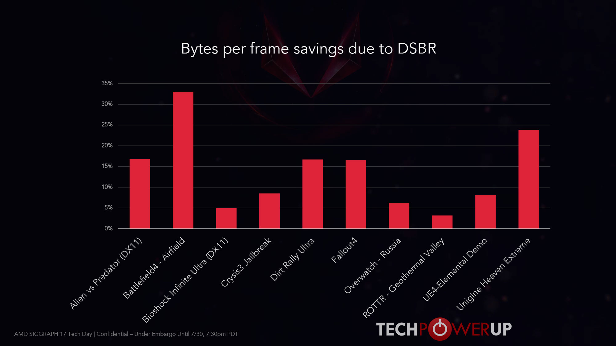
So, I'm not surprised to see that gaming performance with Vega FE is hobbled by both immature power management and inactive DSBR.
Why do we have slides like this if DSBR is inactive?
slides-43.jpg
 
Isn't it $700 vs $699?
Regular RX Vega is $500. Or $600 to anyone who thinks an aluminum shroud is somehow worth $100 more (though AMD may pull a nvidia and only sell founders limited editions during the first month or so).


Why do we have slides like this if DSBR is inactive?
It's inactive in current Vega FE drivers. It'll be enabled on time for RX Vega release, which is what these slides are about.
 
Last edited by a moderator:
The wafer shot does have some portions where the RBE sections are well-lit. They seem mostly free of large arrays.
I would think that the rasterizer would mostly interact with depth information, which is something like 4KB per RBE in Hawaii. AMD's been pretty consistent with RBE caches with GCN, and GCN's counts seem to be consistent with GPUs prior.
Even if significantly larger, it's starting from a very low point and AMD may be counting on the L2 to mitigate any capacity needs from now on.
Yeah. AMDs ROP caches (CB and DB) have been historically quite small. But Nvidia also doubled their L2 when they moved to tiled rasterizer. And I would guess than AMDs 64 wide waves prefer bigger tiles than Nvidia's 32 wide warps (assuming you need to find 16 quads with the same shader in the same tile to fill the wave fully). I would guess that we are talking about tile sizes of at least 128x128, thus depth tile (32 bpp) >= 64 KB. Color tile (RGBA16f) >= 128 KB. But that 2 MB increase in L2 size should be enough for these purposes. L1 ROP caches can remain as tiny as AMDs previous ROP caches.

But how much storage does the binned geometry need? Let's pick some triangle count, for example 8192 triangles. Let's assume roughly 1 vertex shaded per triangle and let's assume 4x float4 interpolants. That's 512 KB of vertex interpolants and 16 KB of vertex indices (assuming 16 bit indices). Is 8192 triangles enough? I would say no, if you want to do proper hidden surface removal. In that case you need much more. But what if they did go one step further, and separated position calculation from the rest of the vertex shader? This only needs float4 storage per vertex, regardless of interpolant count. In this case, you could also do HSR in the binning step, only emitting those triangles that cover pixels. This would allow you to run full vertex shader only for those triangles that have at least one visible pixel. It would also have similar effect as "z-prepass" for pixel shader culling (as the binning step would generate the partial depth buffer for the tile). I did some experiments with a compute shader based pipeline like this. Could be really efficient if done at hardware level.
 
Yeah. AMDs ROP caches (CB and DB) have been historically quite small. But Nvidia also doubled their L2 when they moved to tiled rasterizer. And I would guess than AMDs 64 wide waves prefer bigger tiles than Nvidia's 32 wide warps (assuming you need to find 16 quads with the same shader in the same tile to fill the wave fully). I would guess that we are talking about tile sizes of at least 128x128, thus depth tile (32 bpp) >= 64 KB. Color tile (RGBA16f) >= 128 KB. But that 2 MB increase in L2 size should be enough for these purposes.
Doesn't 64 wide waves also require more L1/L2 for the temporary data generated between graphics pipeline stages?
 
The problem with this bundle is to get the 100 dollars savings you have to purchase the most expensive AMD motherboard as each of those MB listed in the promo is the top of the line MB from Asus, gigabyte and MSI, you also have to buy more expensive 8 cores(can't buy a ryzen 1700), to qualify for the bundle.

One could save more on their own by building their own bundle and not picking these more expensive parts.
 
  • Like
Reactions: xEx
Isn't it $700 vs $699?

Regular Vega is $500. Limited Edition is $600 with a bundle and $699 is the water cooled bundle.

The bundles are 2 games + $100 off Ryzen combo + $200 off Samsung monitor. One of the sites said more options (at least monitor) were coming soon
 
In this case, you could also do HSR in the binning step, only emitting those triangles that cover pixels. This would allow you to run full vertex shader only for those triangles that have at least one visible pixel. It would also have similar effect as "z-prepass" for pixel shader culling (as the binning step would generate the partial depth buffer for the tile). I did some experiments with a compute shader based pipeline like this. Could be really efficient if done at hardware level.
The most recent description from some of AMD's patents has screen space subdivided into some number of rectangles.
When the rasterizer is deferring shading, a triangle's initial bin is determined and it then enters that bin's list of primitives. This then begins by querying how many tiles it intercepts along one axis. The max and min intercepts are recorded, and the bin will accumulate primitives until full or some other condition is hit.
Then, the list of additional intercepts is passed onto another query step that gets the max and min of bin IDs along the other axis in screen space.
After that reaches some closure condition, the hardware concludes its intercept determination and starts to evaluate coverage.
Within a bin, pixel coverage is determined and what primitives belong to each pixel in a tile are recorded with potentially some number of multiple IDs per pixel allowed in the presence of transparency. There's mention of a possible way of continuously updating a batch so that it can dynamically remove primitives while accumulating more, which may allow more coalescing by preventing culled IDs from hitting the maximum bin size, although it's unclear if that is implemented (would require some kind of indirection to the indices, perhaps?).
The context associated with interpolation and resources associated with export buffers and pixel data may count towards batch closure conditions.

Then there is the number of primitives per batch, which yields a size of the primitive ID for the buffer--needed for coverage and the order of shading.
Then, there's some additional context like whether a primitive is opaque, some flags for the stage of processing a batch/bin is in, some form of depth information per pixel, and an output of coverage either by the scan converter or at that level of precision.
AMD posits for the purpose of utilization at least double-buffering all of this, so multiples of some of the context are to be expected.

8192 primitives per batch is 13 bits per primitive, the number of rows and columns can attach 4 additional fields as form of pipeline context that would take up storage even if not used in the data passed to pixel shader launch.
The tile size is going to give ID bits, transparency, depth of the closest occluder, and some number of IDs per pixel.
There's in effect, an ID buffer of 128x128 pixels with at least 13 bits per pixel without transparency.

With the ID alone, it's 26KB to just express for one tile what primitive goes to a pixel without double-buffering, transparency, or higher sampling level. Perhaps the depth for the tile can be shared between batches in a double-buffered setup?
 
And the bundled FreeSync monitor apparently has the reputation of being one of the worst FreeSync monitors in terms of flickering (to the point where Samsung recommends in their manual not to enable it.)

It's solved. Most probably solved by default in the RX Vega launch driver too, since it's a simple misdetection of the screen's horizontal frequency by the driver.
There's no such thing as Samsung recommending FreeSync to be disabled, either.


Nice try at lurking reddit for FUD defects on the bundle, though.
 
So texture sampling returns packed results to GPRs. This seems to imply that 8-bit and 16-bit texture sample operations will return as packed results in unsigned integer (four or two results packed into one register), and then uses shader instructions to read the results out of the register and converting to fp32 at the time of being used. If true, this should save register space compared with loading texturing results directly into VGPRs as fp32 values (ALU cycles are cheaper than VGPRs).

The new addressing instructions might also lead to reduced VGPR usage. Now, instead of having source values for address calculation (which can't be discarded straight away) plus the register allocation for intermediate values in a sequence of address computations, these new instructions would increase the chances of going from source values to address without needing intermediates. Well, that's my theory.

The 8-bit operations (sum of absolute differences) are ancient instructions, not sure why they're being mentioned now.

The "explanation" of the primitive shader is entirely unconvincing. Seems likely to be a white elephant. I wonder if this was built by AMD as the basis for a console chip at some later date. In a console it would be totally awesome, I presume.

---

How much of Vega's (and Polaris's?) power problems are solely due to Global Foundries, versus TSMC?
 
So all you need to do is to hack the video timings? Awesome! :)
I guess the point is there's nothing wrong with the monitor and a driver update will fix.

This thing has a 80-100 freesync range? That's not much....
 
I'm wondering, where all this goes. Maybe we can put the pieces together. The most obvious ones:
- 4 MiByte L2-Cache
- 64× 64 kiB LDS
- 64× 4 KiB Scalar RF from Siggraph arch preso, GCN whitepaper says 8 kiB sGPRs
- 64×4×64 KiB Vector RF
- 64× 16 KiB L1-Cache

If I'm not mistaken, that's 25856 KiByte only.

Possible additions so far - without actual sizes though:
- HBCC buffers
- ROP Caches (4 kiB per RBE?)
- Parameter Caches
- Constant Caches
- DSBR-Tile-Cache
- Color Cache per RBE (was 16 kiB in Hawaii)
- Z-/Depth-Cache per RBE (was 4 kiB in Hawaii)
 
Last edited:
I guess the point is there's nothing wrong with the monitor and a driver update will fix.

This thing has a 80-100 freesync range? That's not much....

It has two ranges in two modes, one is 80-100 and the other is 48-100.

Honestly no idea why samsung does the multiple modes when other vendors using the same panels don't, because yeah, 80-100 is very small. Would be interesting to see the technical details of why they use two .
 
Back
Top