PowerVR Series 6 now official

Information is secure.
PowerVR GPU based on 2 vec4 + additional scalar - 4x2+1 = 9.
Now 9 ÷ 8 = 1.125 bonus!
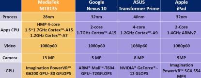
Each core has 2 ALU.
PowerVR G6200 contains 16USSE2 (x2 SGX554).

Now 16USSE2 x vec4 x 2 ALU x 2 Core x 1.125 x 0.280MHz ( mhz for MediaTek) = 80GFLOPS.

By simply :

16USSE2 x 2 Core x 0.280 x 9GFLOPS = 80GFLOPS

See more about calculating PowerVR GPU here :

http://www.359gsm.com/forum/viewtopic.php?f=127&t=13396
I'm not an expect on PowerVR nomenclature, so feel free to correct me, but as I understand it USSE is basically a loose term that refers to all the ALUs in a Series5/5XT core. The SGX535 has 2 ALUs and that was an USSE. The SGX540 has 4 ALUs and that was also an USSE.

In an USSE2, each ALU is capable of executing 1 vec4 MAD and a scalar. The 9 FLOPs/ALU comes from a MAD being 2 FLOPs (4 MAD * 2 FLOPS/MAD +1 scalar) not it being capable of 2 independent vec4 + a scalar. So a SGX543MP2 has 2 cores, each with 1 USSE2, with each USSE2 having 4 ALUs, with each ALU having a vec4 unit and a scalar unit. The iPad 2 is usually calculated to be 16 GFLOPs via (2 cores * 4 ALU * 4 MAD/ALU * 2 FLOPS/MAD * 0.25 GHz clock speed) with the scalar unit not usually included in calculations.

PowerVR hasn't said that the USSE2 is being reused in Rogue. In fact, they've indicated Rogue is using scalar ALUs rather than the vector ALUs in the USSE2. Combined with you using the USSE2 term in to refer to a 9 FLOP Series5 XT ALU, I'm not sure what to make of your Rogue calculations.

There are principles and facts!

2x4+1 = 9GFLOPS! How will you deny this?

PowerVR SGX543 MP1 contains 4USSE2 (SIMD) ! How will you deny this?
PowerVR SGX554 MP1 contains 8USSE2 (SIMD) ! How will you deny this?
All SGX contains 4 MAD'S per SIMD! How will you deny this?

Now is Easy :

Apple A5 - SGX543 MP1 = 4SIMD x 1 Core x 0.200 x 9 = 7.2 GFLOPS!
Apple A6X - SGX554 MP1 = 8SIMD x 1 Core x 0.280 x 9 = 20.16 GFLOPS!

PowerVR Rogue = 16USSE (SIMD) per 1 Core! 4 MAD's per SIMD!
 
Considering he's been spamming this thread repeatedly he's probably just trying to get editing right asap.

Apart from that yes the Series5XT cores consist of Vec4+1 ALUs where the "1" probably stands for a SFU unit, thus giving in total 9 FLOPs per ALU. Still 1 MADD or 2 FLOPs/ALU lane. However Series6/Rogue is a whole new generation of GPUs.

Let's document it a few things again:

http://withimagination.imgtec.com/index.php/powervr/powervr-g6630-go-fast-or-go-home

PowerVR Series6 'Rogue' cores deploy a pipeline cluster approach, with each GPU core scaling up to 8 clusters, and each cluster containing up to 16 pipelines.
Considering they've stated also elsewhere that ALUs are "scalar" this time, 16 "pipelines" stands for SIMD16.

http://www.imgtec.com/news/Release/index.asp?NewsID=666

The first PowerVR Series6 cores, the G6200 and G6400, have two and four compute clusters respectively.
The only thing they don't state anywhere is that each ALU lane is most likely capable of 2 FMACs and therefore 4 FLOPs/ALU lane/clock.

Else:

G6200@MT8135 = 2* SIMD 16 * 4 FLOPs * 0.286GHz = 36.60 GFLOPs

and that is approximately 4x times the FLOP value of a the SGX544 in the MT8125:

http://withimagination.imgtec.com/i...ervr-series6-gpus-to-a-mobile-device-near-you

Thanks to the PowerVR G6200 GPU inside the MT8135 application processor, MediaTek brings high-quality, low-power graphics to unprecedented levels by delivering up to four times more ALU horsepower compared to MT8125
http://withimagination.imgtec.com/i...a-mobile-device-near-you#sthash.tnxVyUbJ.dpuf
 
Ailuros, everything is right, I said it long ago, but wrong in arithmetic :

POWERVR ROGUE -> 2x4+1

1. PowerVR G6100 :

16USSE2 x 1 Core x 0.280 x 9 = 40.32

2. PowerVR G6200/G6230 :

16USSE2 x 2 Core x 0.280 x 9 = 80.64

3. PowerVR G6400/6430 (iPad 5) :

16USSE2 x 4 Core x 0.280 x 9 = 161.28

4. PowerVR G6600/6630

16USSE2 x 6 Core x 0.280 x 9 = 241.92

Cheers!

As ltcommander.data above said USSE2 stands for the ALUs in Series5XT; your math above is off base too since you INSIST to muliply with 9 FLOPs which is Series5XT material but NOT for Rogue.

Again you have 2 FLOPs per ALU lane on Series5XT:

SGX544 = 4 Vec4 ALUs

For each vector ALU lane above you get 1 MADD ie 2 FLOPs * Vec4 = 8 FLOPs + 1 MUL from the SFU = 9 FLOPs in total for each "Vec4+1" ALU.

How bout a KISS approach?

xxxx x (9 FLOPs/clock each)
xxxx x
xxxx x
xxxx x + 2 TMUs


SGX544MP1@286MHz in MT8125:

4 ALUs * 9 FLOPs * 0.286GHz = 10.296 GFLOPs

So far so good but that has nothing to do with any Rogue.

------------------------------------------------------------------------------------------------------------

G6200/6230

2 * SIMD16 clusters * 2 MADDs or 4 FLOPs/ALU lane * 0.286GHz = 36.64 GFLOPs

G6400/6430 = twice as much, G6630 3x times as much at the same frequency.

KISS approach for G6200

xxxxxxxxxxxxxxxx + 2 TMUs (64 FLOPs/clock each)
xxxxxxxxxxxxxxxx + 2 TMUs
 
As ltcommander.data above said USSE2 stands for the ALUs in Series5XT; your math above is off base too since you INSIST to muliply with 9 FLOPs which is Series5XT material but NOT for Rogue.

Again you have 2 FLOPs per ALU lane on Series5XT:

SGX544 = 4 Vec4 ALUs

For each vector ALU lane above you get 1 MADD ie 2 FLOPs * Vec4 = 8 FLOPs + 1 MUL from the SFU = 9 FLOPs in total for each "Vec4+1" ALU.

How bout a KISS approach?

xxxx x (9 FLOPs/clock each)
xxxx x
xxxx x
xxxx x + 2 TMUs

SGX544MP1@286MHz in MT8125:

4 ALUs * 9 FLOPs * 0.286GHz = 10.296 GFLOPs

So far so good but that has nothing to do with any Rogue.

G6200/6230

2 * SIMD16 clusters * 2 MADDs or 4 FLOPs/ALU lane * 0.286GHz = 36.64 GFLOPs

G6400/6430 = twice as much, G6630 3x times as much at the same frequency.

KISS approach for G6200

xxxxxxxxxxxxxxxx + 2 TMUs (64 FLOPs/clock each)
xxxxxxxxxxxxxxxx + 2 TMUs


Agree for Rogue! Convince me! ;)

Corection :

1. PowerVR G6100 :

16USSE2 x 1 Core x 0.286 x 8 = 36.6

2. PowerVR G6200/G6230 :

16USSE2 x 2 Core x 0.286 x 8 = 73.2

3. PowerVR G6400/6430 (iPad 5) :

16USSE2 x 4 Core x 0.286 x 8 = 146.4

4. PowerVR G6600/6630

16USSE2 x 6 Core x 0.286 x 8 = 219.6

Cheers!
 
Convince you of what, for crying out loud? You're not even willing to listen and you apparently have also a hard time reading and understanding public documentation. There are no "cores" in so far announced Rogue variants; from 6100 up to 6630 those it's all single core GPU IP. If you can finally comprehend that and on top of that learn how to count FLOPs per cluster for any Rogue variant then fine we might have made some progress. In the meantime I'm not going to repeat the same stuff over and over again because it doesn't want to sit in your reasoning or you want to increase your post count.

At 286MHz it's per variant as follows:

G6100 = 18.3 GFLOPs
G6200/6230 = 36.6 GFLOPs
G6400/6430 = 73.22 GFLOPs
G6630 = 109.82 GFLOPs

64 FLOPs/cluster for all.
G6100 64 FLOPs * frequency
G6200 128 FLOPs * frequency
G6400 256 FLOPs * frequency
G6630 384 FLOPs * frequency
as simple as that...

Your problem probably is that you haven't realized how low cost Mediatek usually goes and it's under that light perfectly understandable that they'll go for something as humble as the G6200 and with such a LOW frequency as 286MHz for what they call a "high end tablet". It'll come at a budget price hence really a budget offering but still "high end" for Mediatek's own metrics.

In any case if you should be missing some FLOPs in the calculations above for "your iPad5 candidate" double the frequency and you have most of them. Apple doesn't design SoCs with single digit $ values as Mediatek.
 
If I recall the marketing correctly Rogue is designed to run at higher clocks circa 575mhz yet the Mediatek lower clock low cost explanation seems reasonable.

So 500mhz+ Apple A7? SoC for ipad5 that is an G6400 could well be on the cards. Whether we see the G6200 for iphone5S and iPad mini 2 could be a possibility. We also have a potential iPhone 5C which maybe A6 based?
 
Speaking of costs, how does licensing cost work out? I guess it would scale with more clusters etc. but probably not twice the fee for twice the performance?
Also if you manage to clock it higher compared to competition I guess that would be free in terms of licensing costs?
 
Convince you of what, for crying out loud? You're not even willing to listen and you apparently have also a hard time reading and understanding public documentation. There are no "cores" in so far announced Rogue variants; from 6100 up to 6630 those it's all single core GPU IP. If you can finally comprehend that and on top of that learn how to count FLOPs per cluster for any Rogue variant then fine we might have made some progress. In the meantime I'm not going to repeat the same stuff over and over again because it doesn't want to sit in your reasoning or you want to increase your post count.

At 286MHz it's per variant as follows:

G6100 = 18.3 GFLOPs
G6200/6230 = 36.6 GFLOPs
G6400/6430 = 73.22 GFLOPs
G6630 = 109.82 GFLOPs

64 FLOPs/cluster for all.
G6100 64 FLOPs * frequency
G6200 128 FLOPs * frequency
G6400 256 FLOPs * frequency
G6630 384 FLOPs * frequency
as simple as that...

Your problem probably is that you haven't realized how low cost Mediatek usually goes and it's under that light perfectly understandable that they'll go for something as humble as the G6200 and with such a LOW frequency as 286MHz for what they call a "high end tablet". It'll come at a budget price hence really a budget offering but still "high end" for Mediatek's own metrics.

In any case if you should be missing some FLOPs in the calculations above for "your iPad5 candidate" double the frequency and you have most of them. Apple doesn't design SoCs with single digit $ values as Mediatek.


Anyway, I think in terms of devices!
I deal with mobile communications.

iPad 5 came out we'll talk.

Apple will bet on quad-G6400. Be sure!
And it will not be more than 280 - 350 MHz, to save battery power.
As can be seen, MediaTek does just that!

G6200 is a DUAL.
G6400 is a QUAD.

Rogue :
Formulа for devices is a : 16USSE2 x Core x MHZ x 9 or 8 GFLOPS =

Apparently you have any formula. Write to Tim Cook :D

Seems not only I maintain this :

eeTimes via MediaTek :

153311_023375.jpg

You're generating an awful amount of noise over a very short period of time. We are not particularly keen on that around these parts. You've just been told that saying Rogue is USSE2 is dumb, and in the very next post you do just that. Keep it up and your stay will be brief.
 
Since a company like Apple or Intel might implement a similar PowerVR core as a company like TI in a die size approaching almost twice the area (yet with obvious benefits to reaching performance/thermal/consumption targets), it's hard to talk about the typical die sizes we might see in Rogue implementations.

Optimized for area (like TI or perhaps MediaTek might do), a higher-end PowerVR core typically targeted a bit above 8 mm^2 in implementation on the process for which it was initially targeted in the SGX and SGX 5XT generation. Rogue has a number of variants that already scale clusters, so I'd assume that, if Imagination had been reading the trends properly for this generation (and indications are that they did), comparable Rogue solutions will be even somewhat larger to where an A7X could see 50+ mm^2 of GPU area on a 32nm and maybe even a 28nm process. Other SoCs would of course be far less extreme.

I actually think a G64x0 based SoC would work in both the next high-end iPhone and iPad, with the frequency being the main difference.
 
From the very limited and superficial view of each demo these YouTube videos give, I have a hard time decisively concluding that Ira is more complex.

The complexity of Ira's skin shaders and other graphical aspects of the model have definitely been reduced from the desktop version, and I can see ImgTec's head also incorporating similar lighting effects like sub-surface scattering and nice skin shaders showing the appearance of pores, blemishes, etc. Still, Ira looks vaguely more complex I guess and should be considering it's being demoed on hardware that's further from release, but the art design of each demo is playing a far bigger role in the appearance of complexity than any subtle technical differences on demonstrations of this level.

Basically, I agree ImgTec did a nice job here yet are probably unnecessarily drawing comparisons to a demo nVidia has thrown a lot of resources and publicity behind.
 
After re-thinking the die area issue a bit, I'd guess that enough die area could be saved from the lack of redundancy in scaling clusters versus cores and in other architectural density improvements in Rogue that A7X's GPU area could be well in line with A6X's.

Still, even though mobile processor and SoC designers are starting to test limits in peak power and heat, I think they have quite a bit more practical headroom to trade off die area for a better balance in performance, thermal, and power, and I expect to see their designs moving in that direction.
 
Ipad 4 has seen a decent (10%) increase in GLB's 2.7 T-Rex test.

Given that unlike Android, no known kernel sources exist in the wild, we can rule out an overclocked kernel;), meaning this improved performance is purely driver related. The latest OpenGL driver is listed as OpenGL ES 2.0 IMGSGX554-97 Anyway, I'm sure this alone is a good sign for Series 6 performance in complex scenes with lots of alpha blending, not even factoring in, the as yet unknown Uarch changes.

http://gfxbench.com/device.jsp?benchmark=gfx27&D=Apple+iPad+4&testgroup=overall
 
Back
Top