Speculation and Rumors: Nvidia Blackwell ...

  • Thread starter Deleted member 2197
  • Start date
Only if Nvidia breaks from their two-level cache hierarchy. My understanding is that Nvidia really tries to avoid the chiplet/tile route for their designs and keep the cache subsystem streamlined even at the cost of compensating it with faster and more expensive GDDR memory. Power consumption might be one of the motivations, since any high-speed interface going off die will degrade power/perf metrics and signal latency. The Infinity Cache implementation in Navi31, while providing more throughput than the previous generation, takes a significant hit in latency.

The question that must be asked, IMO, is at what point (if there is one) does it become more power cost effective to have a relatively small (relative to main memory) amount of off chip (chiplet) SRAM serving as a last level cache versus significantly larger pool of increased speed main memory which would consume more power than a slower pool of main memory?

Is what NV are doing by remaining monolithic with reliance on faster memory (thus more reliance on fast and more power hungry traces as well as faster memory which consumes more power) a design choice around saving board power costs or a design choice about simplifying the design and monetary cost of the GPU?

It's not like we have an apple to apples comparison in the wild to say that monolithic with the fastest main memory possible is necessarily a win over chiplet with slower main memory. We can't exactly compare NV to AMD for this as their GPUs are designed around 2 different design philosophies with some overlap. It's possible that NV keeping memory amounts low in comparison to competing AMD products isn't purely due to monetary cost but power consumption costs as well.

Regards,
SB
 
Only if Nvidia breaks from their two-level cache hierarchy. My understanding is that Nvidia really tries to avoid the chiplet/tile route for their designs and keep the cache subsystem streamlined even at the cost of compensating it with faster and more expensive GDDR memory. Power consumption might be one of the motivations, since any high-speed interface going off die will degrade power/perf metrics and signal latency. The Infinity Cache implementation in Navi31, while providing more throughput than the previous generation, takes a significant hit in latency.

I'd say they're just really slow to chiplets. I doubt they care how much power they save versus cost, they never have before except as a PR stunt. SRAM doesn't scale basically at all anymore, so their giant cache is an absolutely immense amount of die area and cost.
 
I doubt they care how much power they save versus cost, they never have before except as a PR stunt.
I really want to give you the benefit of the doubt that this is a genuinely held belief, but if so, I'm struggling to understand what it's based on? Can you give a concrete example?

NVIDIA's power efficiency has been market leading since Maxwell as far as I can tell. Before Maxwell, they were clearly behind against mobile GPUs and often also behind AMD (Kepler was a big improvement but not enough). It's somewhat ironic that they left the smartphone market with Tegra just before Maxwell, which seems to have given some people (including insiders at ARM/PowerVR...) the mistaken impression that mobile GPUs are magically way more power efficient than NVIDIA. They are not (consider the fact that some NVIDIA laptop GPUs are extremely competitive with equivalent Apple GPUs). And as DegustatoR said, power is performance when you are TDP limited, which is true for most notebooks, datacenters, and ultra-high-end desktops.

There's a separate question of whether NVIDIA optimises *specific SKUs* for power efficiency - as long as they beat AMD, maybe they don't bother and optimise desktop SKUs more for cost/performance than power, while keeping the most power efficient bins of the same chips for notebooks/datacenters.

One example I noticed just last week is that my RTX 4090's mininum voltage is 0.880v which insanely high for a 4nm chip (at least for me coming from a mobile GPU architecture background) and actually worse than the RTX 3090 so you get a lot less power benefit from clocking below ~2.2GHz than you might expect. It turns out this is a limitation of the SKU and not of the chip itself, as mobile AD10x can go below 0.65v. I assume this is a way to reduce costs for the power circuitry, and/or to increase the expected lifetime endurance of the chip/board, and/or to improve yields for those chips that need a higher Vmin for some reason, but I'm not sure (it could be a completely artificial constraint to hurt their usage in datacenters but that seems unlikely since it wouldn't really help much with that anyway).

Even though H100s are so expensive that the lifetime energy(/cooling) cost of running them in a datacenter is significantly less than the cost of the board/system as far as I know, NVIDIA still has a very strong incentive to maximise power efficiency so that you can have as many of them as possible in a datacenter of a given size.
 
February 27, 2024
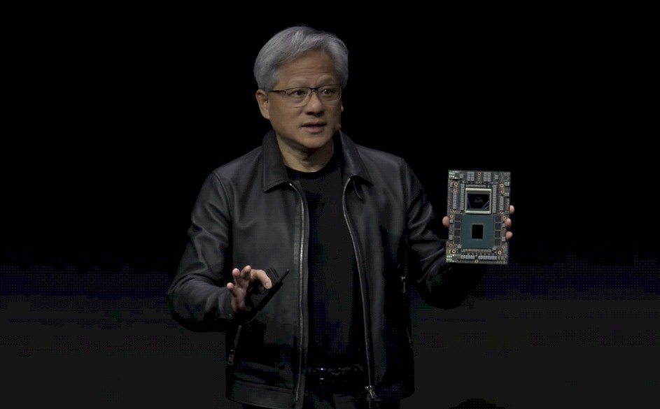
It was clear last August that Nvidia would be a big customer for these chips, and the word on the street is that this 24 GB HBM3E memory from SK Hynix will be used in the impending “Blackwell” B100 GPU accelerators. If so, that would yield 144 GB across six memory controllers on a Blackwell GPU chiplet, and if the B100 package has two GPU chiplets as expected, that would mean a maximum of 288 GB of capacity with 13.8 TB/sec of bandwidth. It is hard to say how the yield would be, and it is possible that only 5/6ths of this is available.
...
It is hard to say what this would cost. It’s not like you can call up Fry’s Electronics and ask what the street price on HBM4 memory is going to be in 2026. For one thing, Fry’s is dead. And for another, we can’t even get a good sense of what the GPU and other matrix engine makers are paying to HBM2e, HBM3, and HBM3e memory now. Everyone knows – or thinks they know – that the HBM memory and whatever interposer is used to link memory to the device are the two main costs in a modern AI training and inference engine.
...
On the street, the biggest, fattest, fastest 256 GB DDR5 memory modules for servers cost around $18,000 running at 4.8 GHz, which works out to around $70 per GB. But skinnier modules that only scale to 32 GB cost only $35 per GB. So that puts HBM2e at around $110 per GB at a “greater than 3X” as the Nvidia chart above shows.

That works out to around $10,600 for 96 GB. It is hard to say what the uplift to HBM3 and HBM3E might be worth at the “street price” for the device, but if it is a mere 25 percent uplift to get to HBM3, then of the approximate $30,000 street price of an H100 with 80 GB of capacity, the HBM3 represents $8,800 of that. Moving to 96 GB of HBM3E might raise the memory cost at “street price” to $16,500 because of another 25 percent technology cost uplift and that additional 16 GB of memory and the street price of the H100 96 GB should be around $37,700.

It will be interesting to hear the rumors about what the H200, with 141 GB of capacity (not 144 GB for some reason), might cost. But if this kind of memory price stratification holds – and we realize these are wild estimates – then that 141 GB of HBM3E is worth around $25,000 all by itself. But at such prices, an H200 “street price” would be somewhere around $41,000.
 
Last edited by a moderator:
That article sounds like it was written by a marketing executive at a DRAM vendor tbh... there's some truth to it but it's wildly overfocusing on memory.

The article says training reaches 80% utilisation (after heavy optimisation - this matches public claims from NVIDIA and others) as if that was terrible and warranted increasing DRAM bandwidth by 11.3x but flops by only 4x. Last I checked, 80*11.3/4 is greater than 100, so they don't actually need the bandwidth, and their argument is wrong.

Generally inference is more bandwidth limited, especially low latency inference where increasing the batch size (to reduce DRAM bandwidth intensity by amortising reading the weights over more samples) cannot be done as aggressively due to latency requirements.

For LLMs specifically, I disagree for training, but I agree with their conclusion for latench-sensitive inference (although this revolutionary paper that just came out might change everything again: https://arxiv.org/abs/2402.17764 )
 
I really want to give you the benefit of the doubt that this is a genuinely held belief, but if so, I'm struggling to understand what it's based on? Can you give a concrete example?

NVIDIA's power efficiency has been market leading since Maxwell as far as I can tell. Before Maxwell, they were clearly behind against mobile GPUs and often also behind AMD (Kepler was a big improvement but not enough). It's somewhat ironic that they left the smartphone market with Tegra just before Maxwell, which seems to have given some people (including insiders at ARM/PowerVR...) the mistaken impression that mobile GPUs are magically way more power efficient than NVIDIA. They are not (consider the fact that some NVIDIA laptop GPUs are extremely competitive with equivalent Apple GPUs). And as DegustatoR said, power is performance when you are TDP limited, which is true for most notebooks, datacenters, and ultra-high-end desktops.

There's a separate question of whether NVIDIA optimises *specific SKUs* for power efficiency - as long as they beat AMD, maybe they don't bother and optimise desktop SKUs more for cost/performance than power, while keeping the most power efficient bins of the same chips for notebooks/datacenters.

One example I noticed just last week is that my RTX 4090's mininum voltage is 0.880v which insanely high for a 4nm chip (at least for me coming from a mobile GPU architecture background) and actually worse than the RTX 3090 so you get a lot less power benefit from clocking below ~2.2GHz than you might expect. It turns out this is a limitation of the SKU and not of the chip itself, as mobile AD10x can go below 0.65v. I assume this is a way to reduce costs for the power circuitry, and/or to increase the expected lifetime endurance of the chip/board, and/or to improve yields for those chips that need a higher Vmin for some reason, but I'm not sure (it could be a completely artificial constraint to hurt their usage in datacenters but that seems unlikely since it wouldn't really help much with that anyway).

Even though H100s are so expensive that the lifetime energy(/cooling) cost of running them in a datacenter is significantly less than the cost of the board/system as far as I know, NVIDIA still has a very strong incentive to maximise power efficiency so that you can have as many of them as possible in a datacenter of a given size.

AMD has equalled or beaten Nvidia in performance per watt quite a few times, RDNA2 was quite competitive with Ampere in terms of efficiency despite higher clocks: https://www.igorslab.de/en/grasps-a...with-benchmarks-and-a-technology-analysis/13/

RDNA3 versus Ada is the exception, not some pattern, thanks to a major power bug that has RDNA3 shooting a good deal under AMD's own projections (which remember, they're legally liable to their stockholders for being honest about) despite their best attempts. The 7900 GRE shows just how bad the yields are.

AMD being competitive is not a belief, just facts outside Nvidia's PR purview. AMD has also found the average GPU consumer cares more about benchmarks by themselves than efficiency, which is nigh certainly true, asking people to do any more math than necessary is a fools errand.

Nvidia would and will happily trade much lower cost for a bit of power efficiency if and when available. The same "cost/efficiency/performance" triangle applies to them as it applies to anyone else. That being said by the time they get to chiplets we'll be seeing hybrid bonding available, so the power penalties will be relatively minimal anyway versus going over solder like AMD does now.
I think RDNA2 was more the exception rather than the rule. If I remember AMD made special effort to come out with more efficient GPUs at the time.
I believe both Pascal and Maxwell were more efficient than their counterparts over the past decade. Before that it may have been different.
 
Last edited by a moderator:
If I remember AMD made special effort to come out with more efficient GPUs at the time.
No?
The thing pushed clocks, and hard, iso node. Not really the sane or straightforward way to gain efficiency (power, that is. Moar clocks is always a win on area).
Before that it may have been different.
Kepler vs GCN was a cointoss depending on the part tier.
 
RDNA2 was quite competitive with Ampere in terms of efficiency despite higher clocks
That's actually against RDNA2 not in favor of it, Ampere is made with much bigger dies on a significantly worse node (Samsung 8nm). So the fact that Ampere managed to tie RDNA2 is something in favor of Ampere, not against it.

Other than that, Maxwell was much more effecient than Fiji (FuryX), Pascal was much more efficient than Vega/GCN5, Turing was more efficient than RDNA1/Vega VII despite being on older 12nm node vs the 7nm of RDNA1, Ampere tied RDNA 2 despite the worse node, and Ada is much more effecient than RDNA3.
 
That's actually against RDNA2 not in favor of it, Ampere is made with much bigger dies on a significantly worse node
Bigger dies that clock lower versus a speed daemon.
The funniest, dumbest N2x part clocked 2.9 or therein.
It's a very fair comparison of Si spam versus speed.
and Ada is much more effecient than RDNA3.
Only because of an oopsie.
Please wait for strixes onegai™ (especially Halo).
So the fact that Ampere managed to tie RDNA2 is something in favor of Ampere, not against it.
Bigger die clocked lower with with a lot more membw to throw around is a fair comparison point.
Either way see e9820 versus sd855 stuff for N7 versus 8LPx derivatives in perf/w benching.

Either way this isn't B100 talk.
Talk B100.
 
Historically AMD and Nvidia have gone back and forth on power efficiency. AMD was generally more efficient from R300 all the way up to GCN. Nvidia was then ahead from Kepler through Turing. RDNA 2 was a temporary switch back to AMD.

Does anyone have any speculation as to what feature or features Nvidia will introduce with the RTX 5 series?
 
Does anyone have any speculation as to what feature or features Nvidia will introduce with the RTX 5 series?
Feature-wise Nvidia seems to keep bringing stuff out of the woodwork (ray reconstruction, RTXHDR) so would not be surprised to see alot of similar in Blackwell.

There is a rumor that the 5090 will be 70 percent faster than the 4090. If true hopefully we can expect some good performance gains in lower tier Blackwell products since mid/low tier will likely be where the most competitive price/performance is found.
This performance boost would likely come from as many as 192 streaming multiprocessors in the RTX 5090 (a 50% increase over the RTX 4090's 128), giving the card 24,576 CUDA cores, 192 ray tracing cores, and 768 tensor cores. In other words, if any of these rumors pan out then this card will be a true behemoth.
 
If true hopefully we can expect some good performance gains in lower tier Blackwell products
Cost per xtor is flat so no, lower end stuff with no margin leeway will have flat-ish perf forever and ever.
You pay more to win more, that's kinda name of the game really.
 
Cost per xtor is flat so no, lower end stuff with no margin leeway will have flat-ish perf forever and ever.
You pay more to win more, that's kinda name of the game really.
I don’t see how the consumer GPU market can continue to exist if this continues indefinitely. There will come a point where enough people get priced out. For example, if the 5090 launches at 2500, where will that price the rest of the stack?
 
Last edited:
I don’t see how the consumer GPU market can continue to exist if this continues indefinitely
The biggest consumer dGP perf/$ bumps always tended to be shrinks sans a few exceptions (remember G92 or R870 or Pascal/Polaris/whatever? good stuff).
We're kinda out of that goodness (assuming flat cost per xtor yielded (and it's not, N3e is more expensive than N4p, for example) you'll be getting like 10-15% perf bumps a shrink optimistically).
There will come a point where enough people get priced out
So far both vendors successfully moved ASPs up a fair bit but I doubt that is sustainable.
For example, if the 5090 launches at 2500 where will that price the rest of the stack?
Depends on die sizes of each part.
Something 200mm^2 N4p will be very much priced like 4060ti.
 
I'm not so pessimistic personally: price per "logic transistor times iso-power performance" is is still going down from N5/N4 to N3E, and chiplets are improving rapidly with better/cheaper packaging tech.

As a hypothetical thought experiment: imagine AD10x but using 3D stacking ala MI300X with multiple N3E top dies and a single N6 bottom die, where the N3E dies are shared across the entire product family and the N6 bottom die is unique per product. The N3E dies *only* have GPCs on them and the N6 die has literally everything else. If you can get dense enough connections (ala Intel Foveros Direct) at a low enough cost, I think this might be a very significant perf/$ improvement versus AD10x even without any other architectural changes once N3E yields are mature enough. So e.g.: 104-equivalent = small N6 base + 1 N3E top, 103 = medium N6 base + 2 N3E top, 102 = big N6 base + 4 N3E top, etc... The other benefit is that multiple 6nm tape-outs would be a lot cheaper than multiple N3E tape-outs, and this doesn't require as big architectural changes as getting the "non-GPC logic" to work across multiple chips, as long as you can afford enough connections between the dies (i.e. this wouldn't work with 2.5D stacking ala RDNA3).

Now... I think it'll happen eventually, but do I believe this is going to happen with Blackwell? Only if it turns out they decide this is also the optimal strategy for their high-end AI chips (to amortise R&D) and there's enough packaging capacity to make it happen in sufficient volume for both AI and consumer somehow. So... very very unlikely!
 
price per "logic transistor times iso-power performance" is is still going down from N5/N4 to N3E
It's up.
It's actually up.
N3e wins you on power/perf but it costs more per xtor which is stinky.
It's a real issue and N2 is even worse wrt that (to the point of majorly influencing packaging decisions for Venice -dense).
As a hypothetical thought experiment: imagine AD10x but using 3D stacking ala MI300X with multiple N3E top dies and a single N6 bottom die, where the N3E dies are shared across the entire product family and the N6 bottom die is unique per product. The N3E dies *only* have GPCs on them and the N6 die has literally everything else. If you can get dense enough connections (ala Intel Foveros Direct) at a low enough cost, I think this might be a very significant perf/$ improvement versus AD10x even without any other architectural changes once N3E yields are mature enough
This is expensive low throughput packaging that's not suitable for mainstream parts.
So e.g.: 104-equivalent = small N6 base + 1 N3E top, 103 = medium N6 base + 2 N3E top, 102 = big N6 base + 4 N3E top, etc...
You're describing the now dead Navi4c.
There's a good reason why this was reserved for only the most expensive things.
Only if it turns out they decide this is also the optimal strategy for their high-end AI chips (to amortise R&D) and there's enough packaging capacity to make it happen in sufficient volume for both AI and consumer somehow. So... very very unlikely!
NV has no experience or any real pathfinding into doing very fancy 3D stuff, it's all Intel and AMD (all things MCM in general are CPU land since many-many decades ago).
Both B100 and N100 are very simple straightforward products (big retsized die times n on CoWoS-L).
 
Back
Top