Nvidia GT300 core: Speculation

Status
Not open for further replies.
It's has been delayed recently..IIRC first mass production (32 nm) won't start before end of 2010.

Here from July TSMC Q2 2009 Conference Call:

Dr Morris Chang:
"On 32, 28, we have had a major effort going for some time now and we are on track in the technology development of 32 28. We have obtained excellent 64-megabit SRAM use and transistor performance for both polysilicon and high K metal gate technologies. We have several customers committed product plans to our 32G and 28 LPT technologies, and new tape-outs will begin in early first quarter 2010.
We also have over 10 customers committed to our 28-nanometer high K metal gate technology platforms and new tape-outs will start in late 2010 and early 2011.
We have also had a large effort started on 22-nanometers for some time now, and we now have a good early baseline of 22-nanometer high K metal gate transistors."

Dr. Mark Liu
"Yes, we are -- we have developed the -- we are approaching the 32, 28 from both approaches. In the end of 2009, we will introduce 32-nanometer with silicon oxy-nitride gate. In 2010, end of 2010, we will introduce the high K metal gate on 28-nanometer. So we think our technology is competitive with IDM technology but most importantly, the 32-nanometer customers already engaged, designs already ongoing. On our 28-nanometer high K metal gate, we have already 10 customers engaged in the designs. So we expect for this customer engagement and future business approach, we are on the same track, on the right track."
So if you assume at the very best will be at least 6 months(yes am way too optimistic) between initial tapeouts and the first products looks like Q3 2010 for 32G products and 28HKMG in mid 2011.

Interesting there was an (unsubstantiated) rumor floating around awhile back the GT3xx derivatives were targetted at 32G. Havent heard anything about any specific AMD products.
 
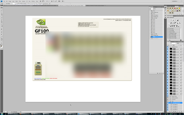
Yep, it's definitely 16 clusters. And it looks like 16 thing-a-majigs in the legend. /shrug.

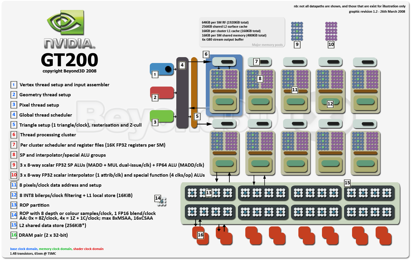
Maybe compare to this:
GT200-full-1.2-26-05-08.png


Edit: Comparing to "GF100" above looks like memory(brown at bottom) is grouped in block of 3 or 6 suggesting 384 or 192 bits.
 
Last edited by a moderator:
Er unless my eyes deceive me in the corner is a legend, a single block containing 16 shaders - and counting there are 2 sets of 8 blocks of these in the main diagram -> 16 x 16 = 256 shaders? That's quite a drop from the original 512

Can almost read the text, just not quite.

..anyone good with photoshop to unblur a little bit?
What if the shaders are double pumped? :p Where do you then end up with.
In my dream
 
Very high electricity bills. They might of course have gone VLIW just like AMD (I think it makes a lot more sense than semi-scalar).
 
Er unless my eyes deceive me in the corner is a legend, a single block containing 16 shaders - and counting there are 2 sets of 8 blocks of these in the main diagram -> 16 x 16 = 256 shaders? That's quite a drop from the original 512

Ah, so it worked... ;)

Quite a drop from what exactly ? Expecting "DX10-ALU's x 2" + DX11 logic "appendages" again ? Not this time.
 
I'm more intrigued by those 4 lonely blue dots and the absence of any SFU looking stuff in that GF100 pic.

Oh, btw rjc - if you want to draw a comparison to the GT200 diagram, that GF100 legend has 32 "dots", not 16.
 
Very high electricity bills. They might of course have gone VLIW just like AMD (I think it makes a lot more sense than semi-scalar).
I am willing to bet that they went wider (32 SPs per cluster) but not VLIW.
 
Oh, btw rjc - if you want to draw a comparison to the GT200 diagram, that GF100 legend has 32 "dots", not 16.
Yes think i was wrong is more likely to be 32 - presently using laptop with shiny screen under fluorescent lighting, lots of reflections, and er headaches.

So 32 x 16 = 512.

Looking at the black rop section above the brown memory interface section, like the memory interface that also appears to be in 3 sections.
 
Looks like 2 16 wide SIMDs per cluster to me. 4 DP FMAs sounds probable but is pretty disappointing (for my purposes, not for games) if true... unless of course you mean that those things are actually 4 DP HW dividers ;).

Could those things be responsible for SFU functions?
 
Random other stuff from picture above:


  • Bottom left has "3.XB transistors, 40nm xx TSMC
  • Second line of text finishes with "fully coherent"
  • Fourth line finishes with "G200 stream output buffer"

If the first item is true is definitely not 256 shaders => must be 512.

Memory interface and ROPs are definitely in groups of 3 or 6....they must have cut the memory interface down from 512 -> 384bits for some reason.
 
Last edited by a moderator:
If you go to the bottom of that page I just linked to at driverhq, and scroll through "This Driver is for these devices", they specifically list "GF100".
 
If you go to the bottom of that page I just linked to at driverhq, and scroll through "This Driver is for these devices", they specifically list "GF100".

Oh dear lord stop it man! it's a rebranded GeForce9300 or the likes. (though the DevID is one up from GT214.)

Code:
<Desc>NVIDIA GT214</Desc>
<HardID>PCI\VEN_10DE&DEV_06B0</HardID>
Desc>NVIDIA GeForce 9300 GE</Desc>
<HardID>PCI\VEN_10DE&DEV_06E0</HardID>

;)
 
Random other stuff from picture above:


  • Bottom left has "3.XB transistors, 40nm xx TSMC
  • Second line of text finishes with "fully coherent"
  • Fourth line finishes with "G200 stream output buffer"

If the first item is true is definitely not 256 shaders => must be 512.

Memory interface and ROPs are definitely in groups of 3 or 6....they must have cut the memory interface down from 512 -> 384bits for some reason.

They probably went with 384 bit memory interface for two reasons: one is the move to GDDR5, which improves their memory bandwith vs prior gen without needing to go so wide; two is the need or desire to have a practical "GX2" style card. Who knows for sure though, hopefully we will find out soon
 
Status
Not open for further replies.
Back
Top