Nvidia Blackwell Architecture Speculation

  • Thread starter Deleted member 2197
  • Start date
You're correct, in that I'm unaware of any die shots of the upcoming chips giving us any idea of the size of the Broadwell options. The PHY limitation is just hypothesis for now, but is an entirely reasonable one.

It may not (only) be that NVIDIA is a bunch of cheap bastards ;)
 
Is there not room around something like AD106 for 6 32bit interfaces? I can't find a die shot of AD106 and the shots I found of AD102 say they're not to scale.

I would think it's unlikely that AD106 doesn't have a 192 bit bus because of design limitations in terms of actually implementing one. It's more likely that decision has considerations for things like cost, power, and product stack reasons.

It's worth remembering that Nvidia sells something like half their discrete GPUs to laptops. Their GPU product stack needs to cater to that as well. The physical and power considerations for 192 vs 128 is likely a bigger factor for that segment than desktop.

It may not (only) be that NVIDIA is a bunch of cheap bastards ;)
But we know it's not strictly a BoM issue for these decisions. Because otherwise it's trivial technically to offer a variant at BoM+margins for double sided (x2) VRAM for all desktop GPUs.

The only reason to not do this is due to wanting to segment the market.
 
But we know it's not strictly a BoM issue for these decisions. Because otherwise it's trivial technically to offer a variant at BoM+margins for double sided (x2) VRAM for all desktop GPUs.

Something technically "trivial" (which is also not necessarily true, because that means design changes and thus more validations) does not mean it's trivial in marketing and retail.
 
I would think it's unlikely that AD106 doesn't have a 192 bit bus because of design limitations in terms of actually implementing one. It's more likely that decision has considerations for things like cost, power, and product stack reasons.
Well, yeah. Which is a design "limitation", i.e. you have to hit some cost of producing a chip for it to sell at a margin you want.

It's worth remembering that Nvidia sells something like half their discrete GPUs to laptops. Their GPU product stack needs to cater to that as well. The physical and power considerations for 192 vs 128 is likely a bigger factor for that segment than desktop.
Both are equally important. A narrower bus usually means higher memory clocks, and it's not a given that such system would consume less power than the one with a wider bus but lower clocks.

But we know it's not strictly a BoM issue for these decisions. Because otherwise it's trivial technically to offer a variant at BoM+margins for double sided (x2) VRAM for all desktop GPUs.
Not sure if I understood this properly: are you saying that putting 2X the memory chips on a card doesn't affect the BOM?
 
Is there not room around something like AD106 for 6 32bit interfaces? I can't find a die shot of AD106 and the shots I found of AD102 say they're not to scale.

AD106 is a strange chip. It’s small at 188mm^2 and barely larger than AD107. They must have been targeting a very specific laptop power profile or something.

They fit 50% more SMs in AD106 and it only increased die size by 18%. That implies all the non-SM bits (memory controllers, front end, encoders etc) are a significant chunk of both dies.
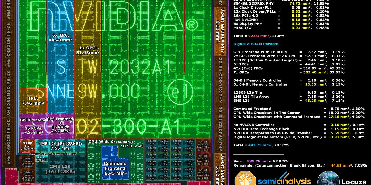
Some numbers (guesses):
1735047814680.png
 
AD106 is a strange chip. It’s small at 188mm^2 and barely larger than AD107. They must have been targeting a very specific laptop power profile or something.

They fit 50% more SMs in AD106 and it only increased die size by 18%. That implies all the non-SM bits (memory controllers, front end, encoders etc) are a significant chunk of both dies.
AD107 is the weirder because it has way less SMs than AD106 and doubling of cache. I mean dies like AD107 are going to become extremely pointless with beefier APUs like Strix Halo's successors and whatever Intel & Nvidia's competitors to them look like. Like AD107 feels so niche and arguably pointless when AD106 could've been cut down (4060 Ti using a full die and then 4060 being a cut down die of it would've made more sense but heh this is Nvidia we're talking about).

Like if all three move onto Chiplet architectures I do expect all three to have a TSMC N3P, N3X etc equivalent node on a monlithic die (say a RTX 70 monolithic 128-bit die on TSMC N3X as the "entry" level card with 4GB GDDR7 Modules so a 16GB SKU or a cut down 12GB SKU) that's maybe AD106 equivalent of maximising compute power in a sub 200mm2 node that can have cut down variants.
Some numbers (guesses):
*snip*
Interesting chart, hopefully a simiar one because I wonder how much that 128MB L2 Cache + Analog will take up GB202 die space in terms of mm2? About 150? 200? 250? I mean 128MB of L2 Cache is probably one of the reasons why Nvidia stuck to an N4P node than N3E (it wouldn't be much smaller, what would be the point? and if RTX 60 is mostly Chiplet based then Nvidia can shave off the cache and analog parts to a cheaper node while the compute gets fancier TSMC N3P or equivalent).
 
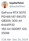
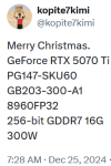
The leaked 5070 config is pretty interesting.

The 4070 super has the same bandwidth and clocks as the 4070 but 10 more SMs, 16 more ROPs and 12MB more L2 at a 20W higher TDP. It benchmarks 15% faster which is pretty good scaling given no increase in bandwidth. That’s 15% higher performance on the super for 10% more power and 21% more SMs. Fair to assume the 4070 super isn’t terribly bandwidth limited.

Now here comes the 5070 with essentially the same number of SMs as the 4070 but 33% higher bandwidth and 25% higher TDP. Why so much more power and bandwidth for the same SM count when clearly neither were necessary to scale up the SM count on the 4070 super? And that’s before factoring in any efficiency tweaks on N4 vs N5.

One explanation could be that GB205 has a smaller L2 and leans on vram bandwidth more than AD104. That wouldn’t explain the power increase though. I think the most obvious answer is that Blackwell SMs are a lot more bandwidth and power hungry than on Ada. Maybe higher clocks. Maybe beefier RT. Or a surprise.
 
I think scalping is more a US problem than an eg. EU problem.

I had never had issues getting a GPU en EU, most sites in eg. Denmark limits how many cards a customer can buy at launch and have effective que systems.
The 30 series launch had a little wait (but no more than 3 weeks), the 40 series I got same week as I ordered.
I think the same appiled to the 20 series, same week delivery.

Yeah funny how it’s impossible to find a simple queue system at US retailers. It’s every man or woman for themselves. So uncivilized.

I had my heart set on a 5090 but $4000 would definitely make me think twice.
 
One explanation could be that GB205 has a smaller L2 and leans on vram bandwidth more than AD104.
Continuing on from my posts about L2 on GB202, it wouldn’t surprise me to see a drop from 8MB to 6MB per 32-bit controller across the line and rely on GDDR7 to pick up the slack. Not sure what the extra room could be used for, though there have long been (weak) rumors of cache changes, possibly a bump to L1 or the register (DSMEM would be interesting even if scaled back). At least with GB202 it seems nearly impossible to keep the same L2/SM ratio as Ada on that die size.
 
Back
Top